From a theoretical standpoint, a low-noise block downconverter (LNB) is a fairly simple circuit. The key components are a pre-amplifier, a local oscillator, a mixer and another amplifier for the L-Band output – that’s it. Now, let’s tear some C-Band LNBs apart and have a look at the practical implementation.
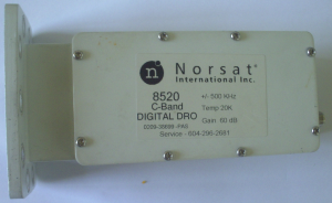
The first LNB I found is a Norsat 8520 C-Band LNB. According to the manufacturer the LNB works between 3.4 – 4.2 GHz with 60 dB gain and has a frequency uncertainty of ± 500 kHz. Essentially ± 500 kHz means that the LO frequency drifts over a range of 1 MHz. That might sound like a lot but is small enough for analogue TV signals.
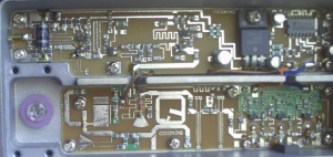
The PCB looks very clean. The design is very straightforward and obviously kept as inexpensive as possible.
On the bottom right is the input pre-amplifer stage. The three white round things with 4 golden legs each are transistors. Right above the transistors (where the green silk screen is) are the bias regulators for the pre-amplifier.
Next there are two 3-pole hair-pin filters. The two band-pass filters are supposed to make sure that only signals in the intended frequency range (3.4 – 4.2 Ghz) make it into the next stage, the mixer.
The mixer circuit is a simple Schottky diode mixer. The rectangular thing in the center of the bottom PCB is a 180 degree stripline hybrid coupler. The stripline on the bottom is the input for the Local Oscillator (LO) signal. On the top right is the input for the RF input (from the 3-pole hairpin filter). The two signals are combined by the hybrid coupler and then handed off to the red Schottky mixing diode. The Shottky diode and the 180 degree hybrid coupler together form a single-balanced mixer. The IF signal (L-Band signal) is then handed off to the top board.
The top board is rather boring: On the top left side is a L-Band amplifier. On the right side is the voltage stabilization for all the circuitry in the LNB.
But wait, we skipped the Local Oscillator (LO) on the bottom board. Let’s have a closer look because this part of the circuit is rather interesting.
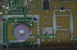
The purple thingy on the far left side (with the transparent plastic screw) is a Dielectric Resonator. A Dielectric Resonator (DR) is an electronic component that exhibits resonance at a particular frequency by means of change in permittivity. In summary, permittivity is a measure of how an electric field is affected by a dielectric medium, in this case the Dielectric Resonator.
Just a little bit to the right of the Dielectric Resonator is the oscillator transistor (white circle with four golden legs). The stripline, which is connected to the left leg of the transistor (transistor’s base), is used to couple the dielectric resonator into the circuit through an electric field.
Dielectric Resonator Oscillators (DRO) can be tuned about ± 20 % around their center frequency by introducing a metallic or dielectric disturbance into the magnetic field [1]. A DRO can be tuned by a voltage if a voltage dependent disturbance is introduced into the electric field. The practical implementation can be as simple as using a varicap tuned stripline.
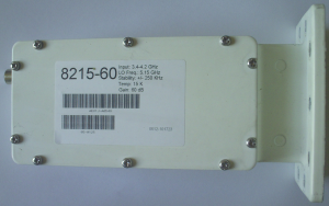
I have another Norsat LNB available for teardown. It’s a Norsat 8215. The main difference is the tighter frequency tolerance of ± 250 kHz. Let’s have a look inside, shall we?
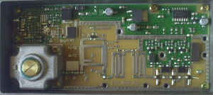
The first difference is that this LNB only has one PCB as opposed to two. The second thing I immediately noticed is the fact that in this design Norsat decided to use three MMICs instead of discrete transistors in the input stage. Also quite apparent is the big heavy metal shielding around the Local Oscillator in the bottom left corner. I would assume that this little shielding case makes the main difference between the ± 500 kHz and ± 250 kHz frequency uncertainty.
Other than that the circuitry hasn’t changed all too much. They’re now using a different type of filter and instead of using just one Schottky diode as in the previous model, Norsat now uses two antiparallel Schottky diodes. In case you’re wondering where the diodes are, they are in the tiny black SOT-23 package above the hybrid coupler.
After removing the metal shield around the DRO, I noticed that Norsat changed the oscillator design a little bit. Now there are two striplines enclosing the dielectric resonator (top and bottom). One stripline is connected to the collector of the oscillator transistor and the other one to the base of the transistor. I personally have very good experience with this kind of DRO and have been using it for many years in homebrew designs.
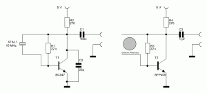
DROs are fairly simple to design. Asides from a few challenges in designing the actual PCB, they have a lot in common with regular Pierce crystal oscillators. Let’s compare a standard Pierce oscillator and an oscillator for dielectric resonators.
The Pierce crystal oscillator is on the left and the DRO on the right side. At first one may notice the ‘missing’ feedback capacitor. But it’s actually there; The parasitic capacitance of the collector-emitter junction. In the GHz range the collector-emitter junction’s capacitance is big enough so that an additional feedback capacitor is no longer needed.
The second difference is that a crystal is actually electrically connected to the circuit. A dielectric resonator is loosely coupled through an electric field between two striplines.
Modern, more stable C-Band LNBs use a 10.05859375 MHz reference Temperature Compensated Crystal Oscillator (TCXO) and a Phase Locked Loop (PLL) based multiplier to generate the 5.15 GHz LO signal. By multiplying 10.05859375 MHz by 512 one gets 5.15 GHz.
Links and Sources:
[1] Properties, Test Methods and Mounting [of Dielectric Resonators], Skyworks: http://www.trans-techinc.com/documents/dr_test_methods.pdf
Westerhold, S. (2012), "C-Band DRO LNB Teardown". Baltic Lab High Frequency Projects Blog. ISSN (Online): 2751-8140., https://baltic-lab.com/2012/09/c-band-dro-lnb-teardown/, (accessed: March 1, 2026).
- Conducted Emissions on the Bench: Implementing the CISPR 25 Voltage Method - December 15, 2025
- WebP-Images without Plugin - January 14, 2025
- Firewall Rules with (dynamic) DNS Hostname - January 14, 2025

Lindsay Wilson
“The purple thingy on the far right side (with the transparent plastic screw)” Should that be “on the far LEFT side”?
KF5OBS
Yes indeed, thank your for noticing and reporting it.
Rakesh
I never knew that DRO’s exist. Good explanation on the parts and their functions.
I have worked with some Bluetooth and AM/FM/DAB receivers. Their RF section is Quite mystical. The Bluetooth 2.0 Antenna consists of two traces in the PCB, placed like a two pronged fork. And the DAB front end has an SMD component (capacitor?) in series to the input RF signal path with the two leads being shorted out by a PCB trace.
While I could appreciate the effect of the capacitance and inductance of the PCB traces at high frequencies, I could not understand the logic behind the PCB trace patterns. Could you give any links or suggested topics to read….
KF5OBS
Rakesh, I am working on a few articles for a new category called ‘microwave circuit design 101’ (MCD101) at the moment. Have a look at the teaser I wrote here; https://baltic-lab.com/2012/10/demystifying-rf-circuit-design-the-art-of-voodoo/
shohel
My signal with 10 ft dish is very low and the elevation is only 5.5 deg, as I m trying to catch apstar 7 from west africa. Previously I used a chinese low cost lnb and could receive only 4/5 c band tv channel. So I bought norsat 8520 r c band (3.7-4.2) because I heard it can reduce terristial interference. But unfortunately I end up with only 2 channels after I installed that new costly lnb….