It took me a while to debate with myself whether or not I should void the warranty on this scope. Curiosity won and I couldn’t resist, I just had to open the box up. After removing the plastic case, a big metal shield is exposed. The metal case is very sturdy and not some floppy budget shield that you see in some of the test equipment around nowadays.
Solid metal cage under the plastic cover
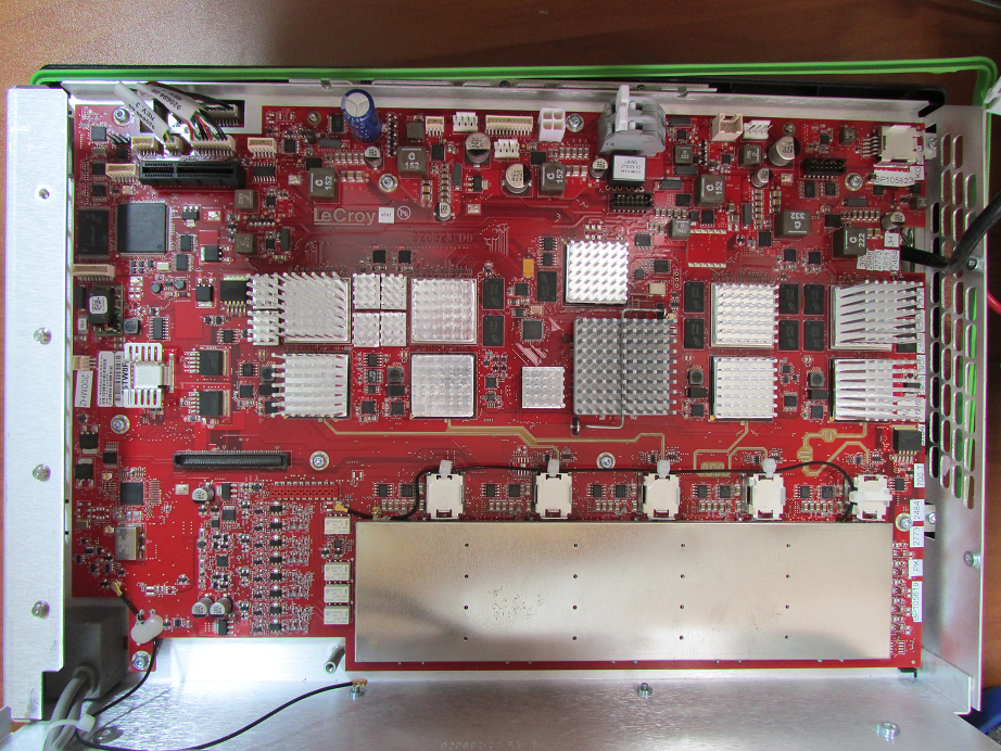
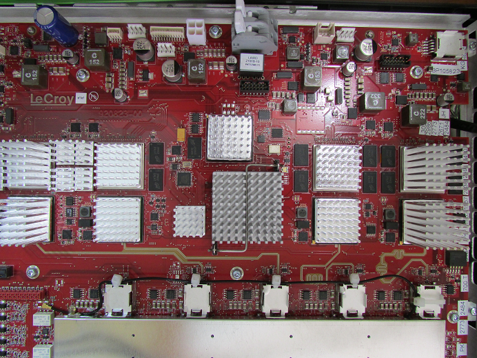
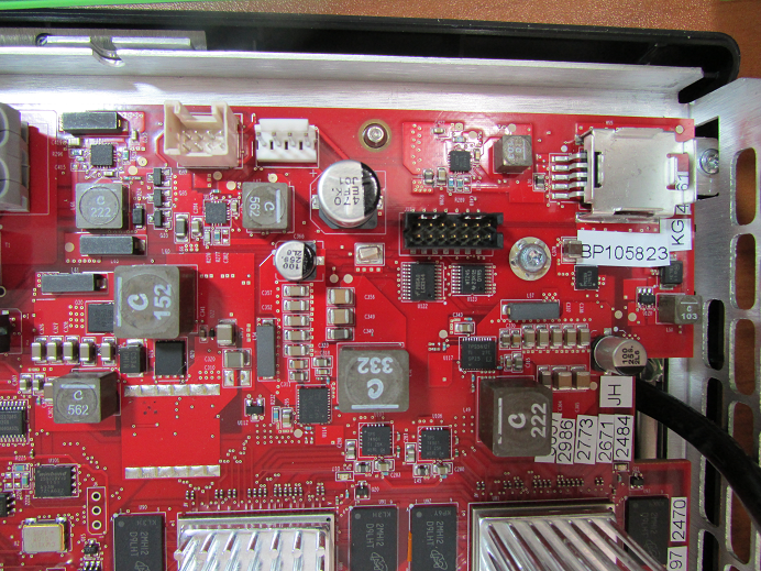
After removing the metal case, the PC side of the scope is visible. I call it the PC side because that’s basically what it is. The scope contains just about anything that you would normally find inside your PC, aside from maybe an optical drive.

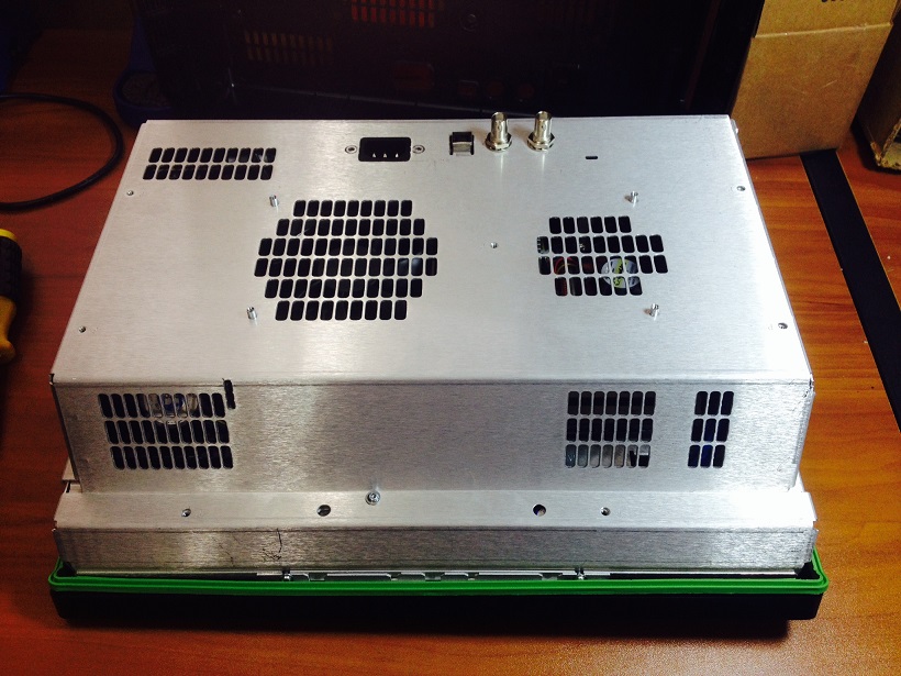
Top view of the opened HDO4024
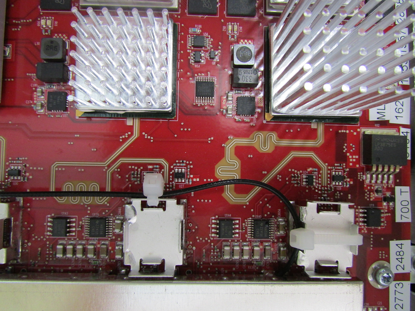
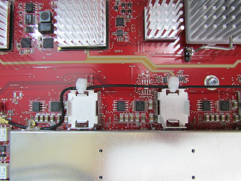
To the right, you can see a standard off-the-shelf PC motherboard. On the left side under the black cover is a switch-mode power supply. The fan in the center brings plenty of air into the acquisition board section of the scope. One thing I noticed immediately is LeCroy’s effort to make everything mechanically stable. Even though in the picture I already disconnected the acquisition board from the top section of the scope, one can clearly see that all cables are mechanically secured and the connectors are well-chosen.
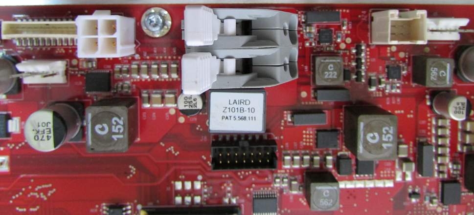
The red PCB in the back carries a few interfaces on the right side and the power mains connector plus a varistor for transient suppression on the left side. The BNCs are the 10 MHz reference input and the external trigger out connectors. Even though it is one solid PCB, there is a clear electrical separation between the peripheral side with a full copper pour on the back side and the power side.
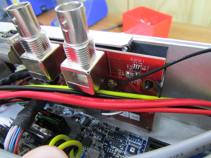
10 MHz reference input (right) and trigger out (left) BNC connectors
The device class USB connector goes straight to the acquisition board.
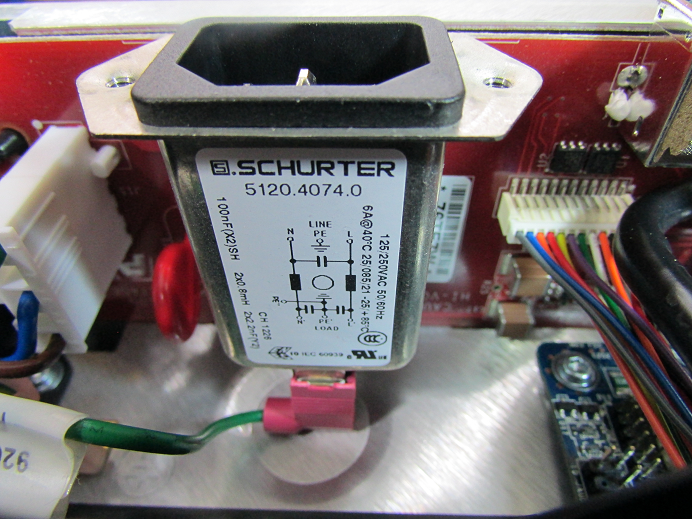
IEC320 power connector with integrated filter
No need to reinvent the wheel on the power filtering side. There are plenty of good IEC320 connectors with integrated filters out there. LeCroy chose a Schurter 5120.4074.0 IEC320 conenctor with inlet filter, available from DigiKey for about $ 8/piece.
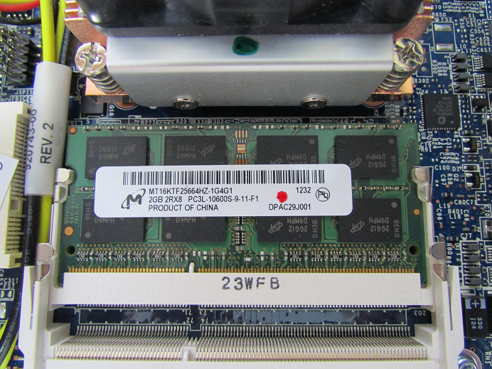
2 GB of RAM
Even though the RAM shows “Product of China” in big capital letters, the manufacturer, Micron Technology, is actually a US-based semiconductor company.
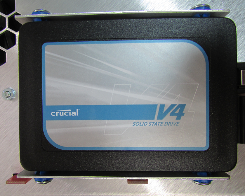
Crucial V4 Hard-drive
Some other manufacturers, like Agilent with their 9000 H-series oscilloscopes, do offer SSDs as a pricey option. I am very happy that the Crucial V4 solid-state drive (SSD) is standard for the LeCroy HDO. Not much needs to be said about Crucial. I mean, Crucial parts are pretty much everywhere you look.
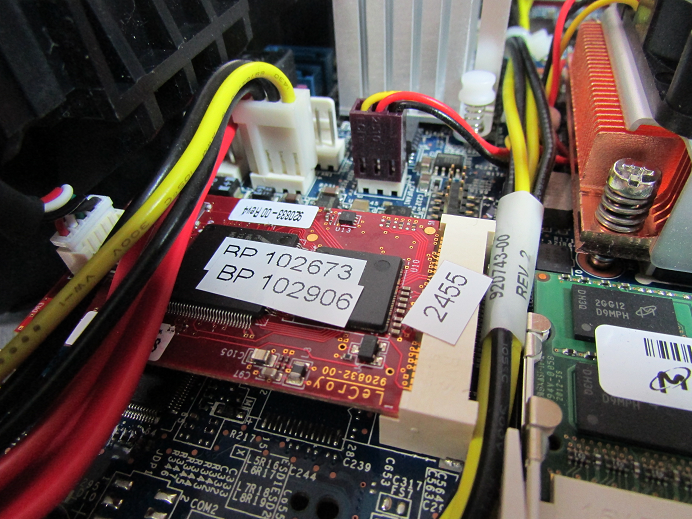
This mysterious board is home to a PLX NET2282 PCI to High-Speed USB 2.0 Controller
The board pictured above looks very mysterious at first due to all the cryptic stickers on them. It turns out to be a carrier board for the PLX NET2282, a PCI to High-Speed USB 2.0 Controller.
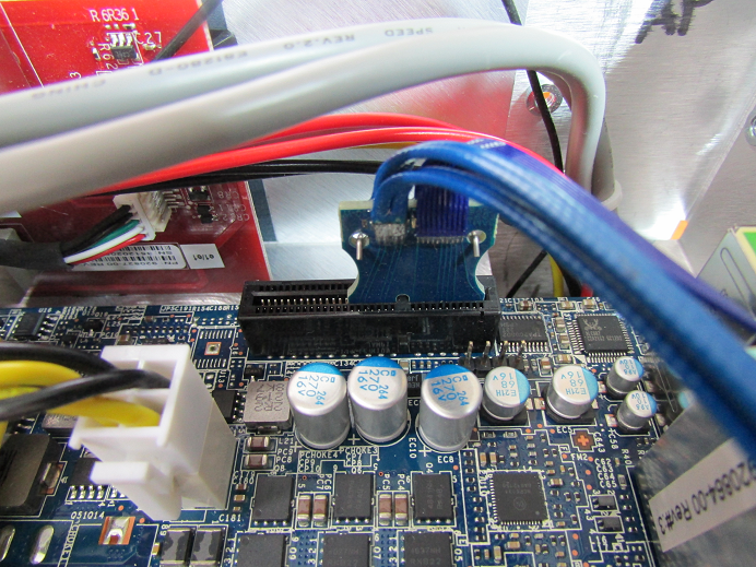
It seems that most of the communication between the motherboard and the acquisition board happens via PCI Express (PCIe). There is a jumper cable from the PCIe slot on the motherboard to a PCIe slot on the acquisition board. Judging by the width of the jumper, only one PCIe lane is used, but that should be plenty of throughput for the scope.
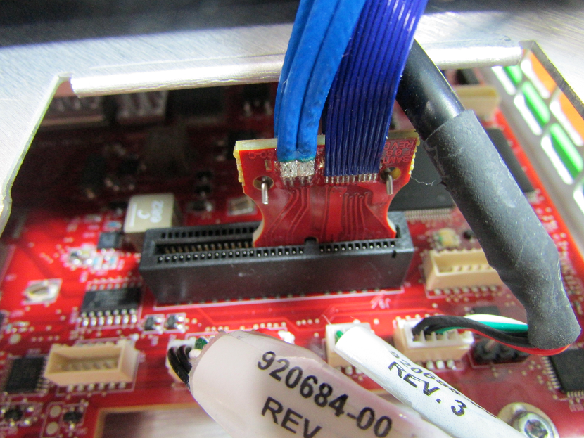
PCIe counterpart on the acquisition board
Even though it’s not captured on the pictures, the PCIe jumpers are mechanically secured with a little clamp. So even though there should be plenty of tension to hold the jumper in place just from the bus connector alone, LeCroy didn’t want to take any chances.
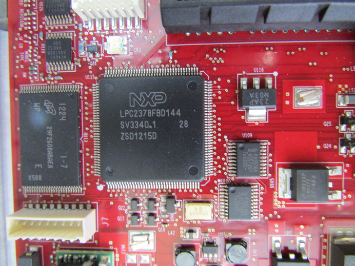
LPC2378 is an ARM7TDMI-S based high-performance 32-bit RISC Microcontroller
The PCIe bus connector on the acquisition board is wired straight up to a NXP LPC2378, an ARM7TDMI-S based high-performance 32-bit RISC Microcontroller. I suspect that microcontroller’s sole purpose is to serve as a PCIe bridge and dispatch data/commands between the motherboard and the acquisition board.
EDIT (10/04/2013): The previous statement can’t be true as the NXP LPC2378 is way too slow to handle PCIe even remotely. Upon further inspection, it appears the PCIe bus is actually connected to the FPGA just above the big ASIC in the center of the scope.
But before I get into details, lets zoom out and get a general overview of the acquisition board.
Overview of the acquisition board
On top of the fact that I really love the red silk screen, I think the board looks very neat and clean. The PCB layout clearly groups the components in functional blocks. The top-center and top-right areas of the board seems to be primarily reserved for power conditioning and power distribution. The top-left corner is host to the PCIe interface and the NXP LPC2378 we talked about earlier.
The bottom-right corner appears to be mostly the domain of clock generation and distribution. I have to admit, I am a bit surprised that the clock section isn’t shielded at all. I am sure the scope is EMC compliant, but at the same time, this looks like an accident waiting to happen where external interference could make its way into the clock generation section of the scope. Teledyne LeCroy may want to revise this and see if my suggestion is relevant for practical applications. While I am writing this, I do remember that I can definitely “see” a 125 MHz (and 625 MHz) peak when using the spectrum analyzer option. Looking at the crystal oscillator’s frequency, it’s apparent where this spike is coming from. Sure, this is an oscilloscope and not a full blown RF spectrum analyzer, but at the same time, this is a high-end piece of equipment. And with 4096 resolution steps, even tiny interference makes it onto the screen somehow.
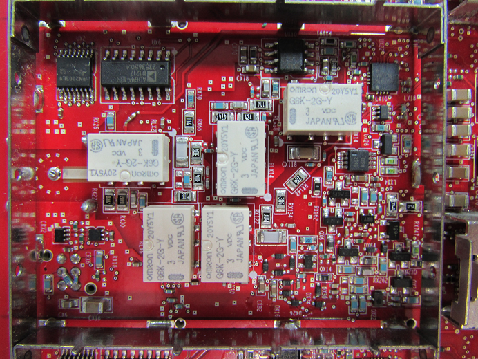
Another overview of the acquisition board
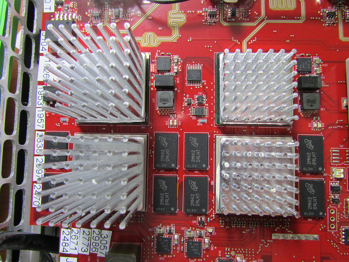
The bottom-center and bottom-right of the board is occupied by a large metal shield. Under the shield, there are 5 front-ends. Why 5 on a 4-channel scope? The fifth is for the external trigger input. It seems that the front-end for the trigger input is pretty much identical to the actual input channel front-ends. But we’ll get to the front-ends later.
Under the 5 metal cans, which are located right above the big front-end shielding, are the ADCs. The first 4 are for channels 1-4 and the fifth one is for the external trigger input. The first 4 ADCs are connected to the FPGAs in the center of the PCB through matched length trace pairs. The kind of ADC used in this oscilloscope is naturally the key element for the scope’s performance. Just as important, however, is the analog front-end.
Big power connector for the main supply
The acquisition board’s main power supply seems to be a single voltage rail. Two big wires feed the single voltage supply into the board’s own power conditioning section.
Power conditioning and an I/O header
In the middle of all the power conditioning elements is a 14-pin header with standard 2.54mm spacing. The connector is wired to a WT245 (4-BIT DUAL-SUPPLY BUS TRANSCEIVER) and a LCX244 (Low Voltage Buffer/Line Driver). I assume this is some sort of programming interface, possibly JTAG or something similar.

A spot for some unpopulated ICs
All over the board I found plenty of little stickers with 4-digit numbers on them. I wonder what they are. I doubt they’re to keep track of parts revisions as you’d expect something like that to be integrated in the silk screen. Maybe employee IDs from the factory identifying who assembled and tested the scope? I guess we’ll never know unless LeCroy lets us in on that secret.
There are also plenty of spots with unpopulated parts. Could it be that they use the same PCB for the HDO6000 series as they use for the HDO4000 series? Either that or the parts were deemed unnecessary and the layout itself is from an older revision. At this point, I may want to mention that my Teledyne LeCroy HDO4024 is one of the first production HDOs leaving the factory. I am sure that since then, there is at least one hardware revision.
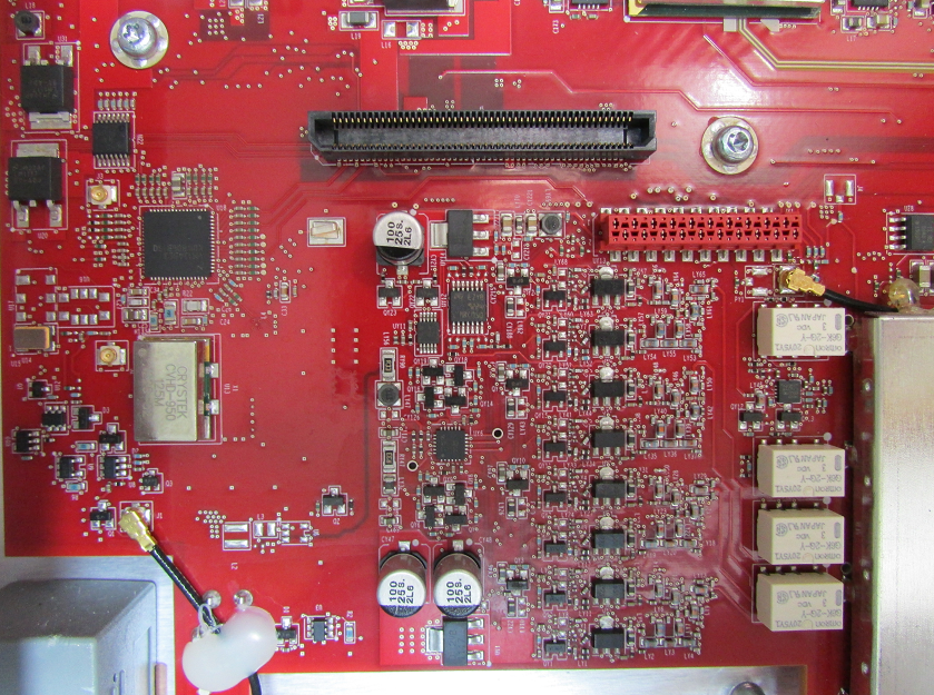
Clock generation and expansion slot
As an RF guy, I of course find the above picture very interesting. It’s the clock generation (left) and clock distribution (right) section of the scope. The little black coax cable is connected to the external 10 MHz reference input. A Crystek CVHD-950 125 MHz VCXO [1] seems to be the scope’s internal frequency reference. Crystek promises an ultra-low phase noise performance of better than -135 dBc/Hz with a distance of 1 kHz to the carrier.
Two expansion slots can also be seen in the previous picture. They are most likely for the planned Mixed Signal option. I am not sure if that option is already in production but I know LeCroy has shown demos of it before.
Channel 2 front-end
Just as important as the ADC is the analog front-end. An ADC is a great “Garbage In/Garbage Out” part. That means if you feed a low-quality signal into it, you’ll have a low-quality output. Therefore, an ADC can only be as good as the analog front-end permits. That was reason enough for me to crack the shielding open to see what’s inside. The left side is where the signal comes in from the BNC and then exits to the ADC on the right.

Channel 1 front-end
I noticed that the front-end of channel 1 looked a bit different from all the other channels. There is a little coax wire from the clock distribution side going into the shielded box connected to a connector that’s soldered onto a trace. It doesn’t really look like the PCB was designed for that connector to be there. This actually does look like a post-production modification. Someone probably messed something up and the LeCroy engineers decided to bodge this little connector onto the PCB.
Looks like someone bodged something onto the front-end section of channel 1
It looks a little ugly, but that’s just how it goes with bodges. As a circuit design engineer I do understand that often modifications need to be made. And electrically this modification is probably great. However, I wish they’d at least clean all the solder flux up a bit. On the bright side, that seems to be pretty much the only real complaint I have about my scope.
ADCs and FPGAs for channels 1 & 2
The defining parts of this oscilloscope of course have to be the ADCs. So what ADCs is LeCroy using? They certainly didn’t make it easy at all to get a glimpse at the part number. The solid metal shielding made it rather difficult to figure out what part it was. My x-ray vision enabled me to figure out, that it is – to my surprise – an off-the-shelf part. The secret is a Texas Instruments ADC12D1600RFIUT [2], an extremely powerful 12-Bit, 3.2 Gs/s RF Sampling ADC. Texas Instruments mentions a steep price of $2399.47 per ADC at a 100 piece quantity. Now obviously, Teledyne LeCroy pays significantly less, but I still imagine the ADCs eat up quite a bit of the budget.
ADCs and FPGAs for channels 3 & 4
Each ADC is connected to an FPGA using matched length differential pairs. It is absolutely imperative that all signals are 100% time-coherent when they make their way from the ADC to the FPGA. Therefore, the wire length between each ADC and FPGA needs to be exactly the same. As the ADCs of channels 1-2 are closer to the FPGAs than the ADCs for channels 3-4, the designers had to make the differential pairs for channels 1 – 2 a bit longer. That’s what the meander pattern is for.
Channel 1 & 2 FPGA section without heat sinks on the SDRAM
If you take a close look, you’ll notice that the SDRAM for the FPGA group of channels 1-2 does not have heat sinks, while the same circuitry for channels 3-4 does. This is not a mistake, though. The cooling fan is situated right above the channel 1-2 FPGA group and can cool this area more efficiently than the channel 3-4 group.
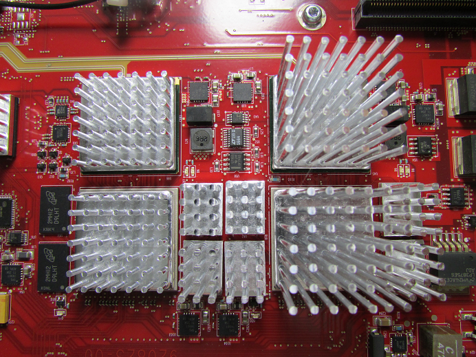
Channel 1 & 2 FPGA section with heat-sinks on the SDRAM

Some sort of ASIC
There’s an ASIC marked “HTT711 38C12” on the board. Judging by its position on the board, I suspect this is the timing and trigger brain of the HDO. Since this is a proprietary ASIC, I have no additional information on this part though.
Alright, that concludes the teardown for now. I am considering making a teardown video. Naturally, video can convey more details than this little post here. If you’d be interested in seeing a teardown video of the Teledyne LeCroy HDO4024 on my YouTube channel, let me know in the comments below!
Update (10/06/2013): Due to the large amount of positive feedback on this teardown, I also made a video of the HDO4024 teardown.
Links and Sources:
[1] CVHD-950 VCXO Datasheet, Crystek: http://www.crystek.com/crystal/spec-sheets/vcxo/CVHD-950.pdf
[2] ADC12D1600 Datasheet, TI: http://www.ti.com/
Westerhold, S. (2013), "Look Inside: Teledyne LeCroy HDO4024". Baltic Lab High Frequency Projects Blog. ISSN (Online): 2751-8140., https://baltic-lab.com/2013/10/look-inside-teledyne-lecroy-hdo4024/, (accessed: March 27, 2026).

- Conducted Emissions on the Bench: Implementing the CISPR 25 Voltage Method - December 15, 2025
- WebP-Images without Plugin - January 14, 2025
- Firewall Rules with (dynamic) DNS Hostname - January 14, 2025
Paul
Hi,
Thanks for going to the trouble of doing this teardown and sharing it.
I’m not sure what to think of upper side of the equipment. (Any clues on who manufactures the PC mainboard?)
The acquisition board looks like some decent work though.
Will be pleased to see the video if you get round to that.
Chris
Video sounds awesome; Great write-up!
Rodney
A teardown video would be great…
Sebastian
Here is the video version of the teardown: http://www.youtube.com/watch?v=QvLHMzSlty4