General Overview
Both the ICS501 and ICS511 are not designed for radio frequency applications. Therefore, they put out square wave signals and the examples given in the datasheets are targeted at typical clock frequencies used in the world of digital electronics. But that doesn’t mean we can’t use them. The two different chips vary in some ways. The IC501 is able to generate multiples of 2, 3.125, 4, 5, 5.3125, 6, 6.25 and 8 for output frequencies up to 160 MHz [1]. The ICS511 has multiplication factors of 2, 2.5, 3, 3.333, 4, 5, 5.333, 6 and 8 up to 200 MHz [2].
I was interested in how these ICs behave with 50 Ohm loads and sources. The nominal output impedance is given in the datasheets as 20 Ohms. In my experiments, however, no apparent signal degradation was observed when using the ICS501 / ICS511 to drive a 50 Ohm load. Unfortunately, the datasheets do not contain any information about the devices input impedance. But it can be assumed that it is rather high. I had no problems feeding a 4 Vpp AC coupled signal directly into the clock input pins of both chips. The chips also didn’t seem to care whether they were supplied a square wave or a sinusoidal waveform. They were happy with either.
Test Circuit
To make my experiments easier, I designed a small PCB with edge mount SMA connectors for clock input and output. I also included footprints for a HC-49 type crystal and corresponding load capacitors. The two solder jumpers can be used to set a fixed clock multiplication factor. The larger through-hole pads that can be seen in the pictures are reserved for future experiments where I will try to use a varicap diode to frequency modulate the output signal. Spoiler alert: Narrow-Band FM using a varicap is possible!
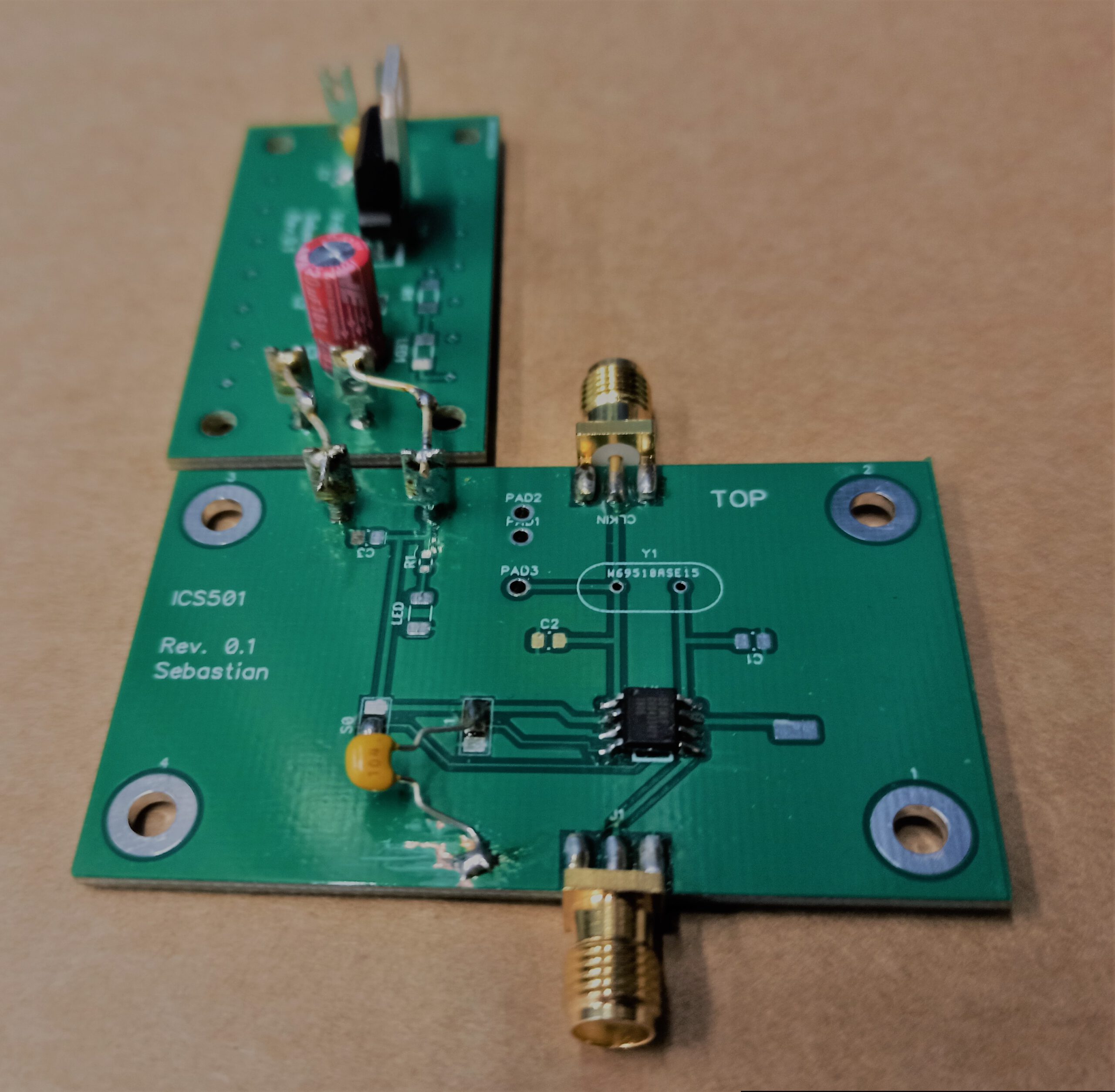
Homebrew breakout board for ICS501 / ICS511 clock multiplier experiments.
The PCB design contains a lot of design errors. But I already designed a Revision 0.2 PCB and send the files of for production. In its present condition, the circuit looks something like this (click to enlarge):
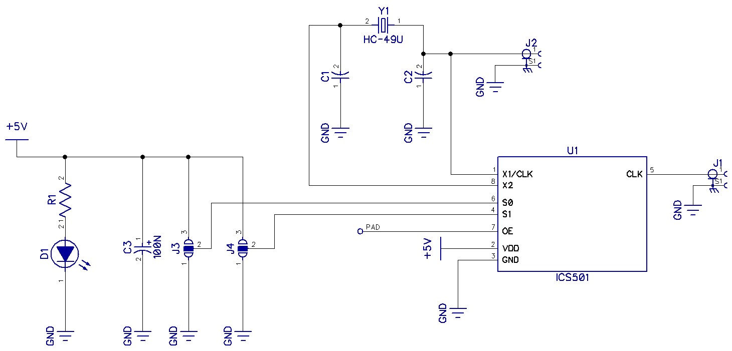
Schematic of the quick and dirty ICS501 breakout board
Test Results
All tests were performed using the ICS501 because I didn’t have any ICS511 in stock. The output signal was fed into a Siglent SDS1202X-E oscilloscope through a 50 Ohm termination resistor.
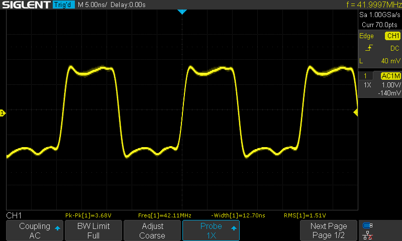
ICS501 output signal, 7 MHz input clock, multiplication factor 6, 42 MHz output signal
The integrated crystal oscillator works well to generate a 144 MHz signal from a 24 MHz crystal. I did not add any load capacitors on the PCB because the internal 12 pF (Source: [ 1], page 3) were sufficient to sustain a reliable oscillation. Frequency accuracy was not important for this test anyway. Note that the now more sinusoidal looking waveform is merely a limitation of my test equipment. The oscilloscope simply doesn’t have enough bandwidth to process the Fourier components (odd-integer harmonic multiples) that give a square wave its shape.
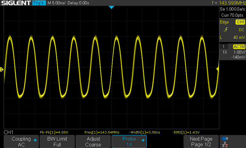
ICS501 output signal, 24 MHz crystal, multiplication factor 6, 144 MHz output signal
Next, I wanted to try what happens if the ICS501 is driven beyond its alleged maximum output frequency of 160 MHz. I was honestly not very surprised to see that the 30 MHz input signal was multiplied to 180 MHz effortlessly.
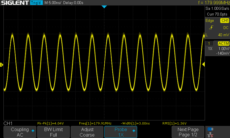
ICS501 output signal, 30 MHz input clock, multiplication factor 6, 180 MHz output signal
The next thing I was interested in was the output spectrum. A 15.1 MHz input signal was multiplied by 6 to generate a 90.6 MHz signal in the FM broadcast band.
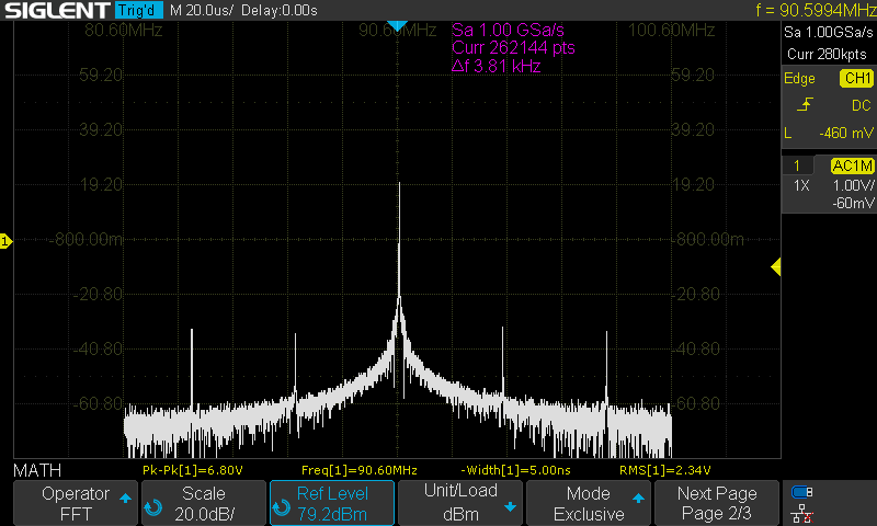
ICS501 output spectrum, 15.1 MHz input clock, 90.6 MHz output. Horizontal scale: 2 MHz / division, vertical scale: 20 dB / division
In the center of the picture we can see the wanted 90.6 MHz signal. But various other peaks spaced a little over 3 MHz from the carrier are also visible. These peaks are calles reference spurs. Their spacing corresponds to the internal frequency used by the phase frequency detector (PFD) inside the ICS501. The exact spacing of these spurs is likely to be 3.02 MHz (input clock divided by 5). The 3.02 MHz is then used by the PFD to lock onto the output signal divided by 30 (90.6 MHz / 30 = 3.02 MHz) to this internal reference frequency. Reference spurs are faily typical for PLL circuits. But nothing to worry about, we can filter those.
If we look at a broader range of the spectrum, more spurs become visible:
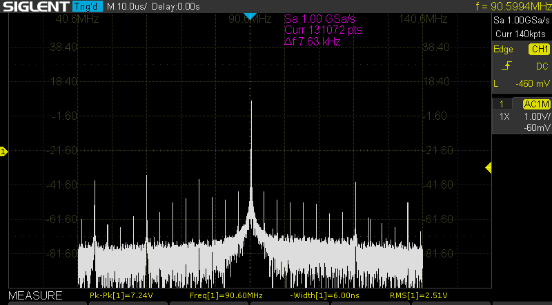
ICS501 output spectrum, 15.1 MHz input clock, 90.6 MHz output. Horizontal scale: 10 MHz / division, vertical scale: 20 dB / division
Besides the aforementioned PFD reference spurs repeating every 3.02 MHz, we can now clearly see even stronger spurs spaced 15.1 MHz on either side of the desired 90.6 MHz center. This is simply leakage of our original 15.1 MHz reference signal.
Conclusions
Altogether I am quite happy with the results so far. These ICs might be a simple solution for generating frequencies in the VHF range from fairly low frequency oscillators, VFOs and standard crystals. Cascading two ICS501 / 511 opens even more possibilities. Especially with standard crystals, the fractional multiplier settings open a foolproof and inexpensive way of generating frequencies that otherwise would require more complicated PLL circuits.
Another interesting application would be to generate extremely accurate clock signals from a standard 10 MHz precision reference source (OCXO, GPSDO, etc.). Stay tuned for more experiments.
NOTE: The ICS501 is considered obsolete / not recommended for new design and chip availability can not be guaranteed. But there appears to be plenty of stock available from large distributors. Certainly enough for the average hobbyist.
Links and Sources:
[1] ICS501 Datasheet, Renesas Wikipedia: https://www.renesas.com/
[2] ICS511 Datasheet, Renesas Wikipedia: https://www.renesas.com/
Westerhold, S. (2022), "ICS501 / ICS501 VHF Experiments". Baltic Lab High Frequency Projects Blog. ISSN (Online): 2751-8140., https://baltic-lab.com/2022/02/ics501-ics501-vhf-experiments/, (accessed: May 7, 2026).

- Conducted Emissions on the Bench: Implementing the CISPR 25 Voltage Method - December 15, 2025
- WebP-Images without Plugin - January 14, 2025
- Firewall Rules with (dynamic) DNS Hostname - January 14, 2025