LDMOS VHF Power Amplifier Prototype
General Overview
For this experiment a single MRF101AN was used. The MRF101AN is suitable for single band PAs on the 6m (50 MHz), 4m (70 MHz) and possibly 1.25m (222 MHz) band. Operation on the VHF broadcast band (88 – 108 MHz) may also be an interesting application for some people. The 2m band (144 – 148 MHz) was selected for initial prototyping and proof of concept. For no other reason than that it seemed the most interesing to me.
The target was an input VSWR of less than 2:1 over the whole frequency range of 144 to 148 MHz. The quiescent current was set to 100 mA as per the datasheet recommendation. The biasing voltage was supplied to the gate via a resistor. From an AC standpoint, the resistor is connected to ground through a capacitor and is part of the input matching network. This is a common technique used in power MOSFET RF design.
Input / Output Impedance Matching
The first step was to match the input impedance of the MRF101AN to the desired 50 Ohms input impedance. According to the datasheet, the input impedance looking into the gate of the MRF101AN should be around 6.2 – j10.2 [1]. A strong capacitive reactance was to be expected given the relatively high frequencies and an input capacitance of 149 pF. The output impedance is given as 9.9 – j5.9. Therefore, it wouldn’t really be possible to use simple broadband transformers for the input / output matching. Since the desired frequency range of operation isn’t very broadband, this isn’t much of a problem.
I elected to use a simple L-Network for the impedance matching. I recommend reading my article on L-Network impedance matching [2]. It should be noted that for reasons of stability, the input of a power MOSFET should never be matched directly to 50 Ohms. The common design practice is to load the gate with a resistor and then match that to 50 Ohms. The output of a power MOSFET on the other hand can be matched directly to 50 Ohms.
The free software SimSmith was used to simulate different component values and simulate their behaviour over the desired frequency range of operation [3]. After trying different component values, I came up with suitable component values for the input matching:
SimSmith simulation of the MRF101AN input L-Network
When these values were tested, nothing seemed to work as intended though. This was no surprise since the prototype was built Manhattan-style. Building a circuit like this Manhattan-style is probably not the most wise design choice. But it certainly is possible. It should be noted that the prototype had a tendency to oscillate between 160 – 170 MHz. The oscillations seized once a bare copper board was placed between the gate and drain sides of the MRF101AN. Additionally, the amount of parasitic reactances threw of my matching circuits. It was apparent that the series inducor was too large. So I grabbed the next smaller size adjustable inductor I had in my parts collection. Now they’re likely too low, but this is just a proof-of-concept protoype. As long as the general circuit works, the exact component values can be adjusted once a proper PCB is designed.
This is the schematic of the “final” prototyping circuit that I used for my tests:

Schematic of the LDMOS VHF Power Amplifier Prototype
MRF101_AN_VHF_Amplifier_Schematic.pdf
Test Results
All simulation and guesswork asided, what really counts is results. Not much effort was put into the testing of the circuit. Just enough to be assured that a PCB with this general topology can be designed and ordered for fürther component value optimization. No tests for linearity and efficiency where performed. For all tests, the quiescent current was set to 100 mA. The prototype was supplied with 50 Volts DC. The output was properly terminated with a 50 Ohm dummyload. A large heatsink made sure that the MRF101AN stayed within its permissible operating temperature range.
The input VSWR of the power amplifier prototype was measured using a properly calibrated Nano VNA. As expected, the input VSWR isn’t perfect. But it is within the design criteria of less than 2:1 over the whole band:

Measured input VSWR of the MRF101AN LDMOS VHF Power Amplifier Prototype
The actual complex input impedance was also measured using the same set-up:
Measured complex impedance of the MRF101AN LDMOS VHF Power Amplifier Prototype
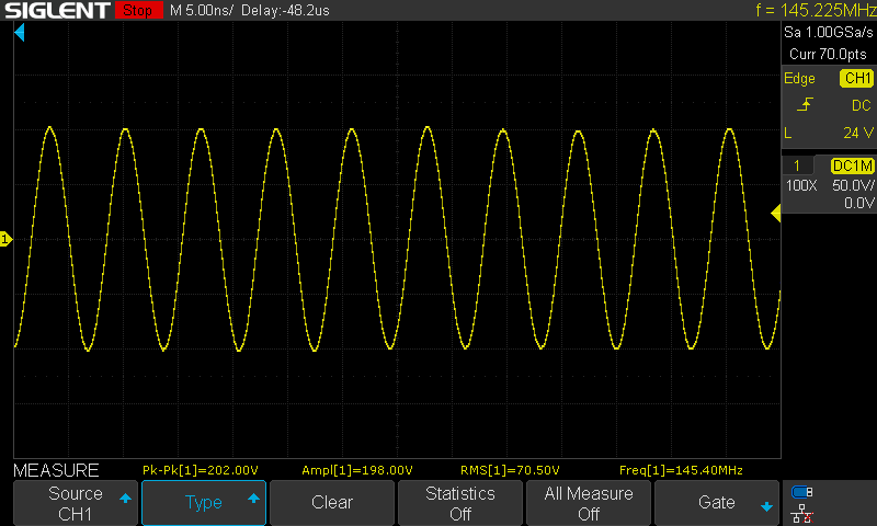
To test the output power of the power amplifier, a simple FM transceiver delivering about 1 Watt of RF power was connected directly to the input of the MRF101AN power amplifier prototype board. A Siglent SDS1202X-E was used to look at the resulting output waveform from the dummyload through a 1:100 oscilloscope probe.
VHF (144-148 MHz) LDMOS Power Amplifier Prototype Test
The resulting measurements would – if true – indicate that an output power of a little over 100 Watts was indeed achieved:
Output of the MRF101AN LDMOS VHF Power Amplifier Prototype
However, the results should be interpreted very sceptically. The measured output waveform appears to be very sinusoidal. But in reality, the signal likely looks very distorted. While the L-Network on the output of the amplifier certainly has a low-pass filter characteristic, not much harmonic suppression canbe expected by it. The oscilloscopes maximum bandwidth of 200 MHz makes it impossible to visialize any harmonic components of the signal. Therefore, the displayed waveform and indicated RMS voltage needs to be interpreted very carefully.
Additionally, the input current into the amplifier prototype was only around 2.3 A. That equates to 115 W DC input power. Assuming 100 Watts of RF output power, the resulting efficiency would be around 87 %. While such an efficiency would surely be impressive for such a simple set-up, it is also highly doubtful. Nonetheless, the dummyload gets noticeably warmer after just a few seconds of full power output.
Conclusions
The results are promising enough to design a PCB layout and continue testing this set-up. Expect a follow-up on this topic.
Also, I would like to get some feedback on whether or not a 4m-Band linear amplifier kit would be of interest for the amateur radio community?
Links and Sources:
[1] MRF101AN / MRF101BN Datasheet, NXP: https://www.nxp.com/
[2] L-Network impedance matching https://baltic-lab.com
[3] SimSMith, Ward Harriman, AE6TY http://www.ae6ty.com/
Westerhold, S. (2022), "VHF LDMOS Power Amplifier Experiments". Baltic Lab High Frequency Projects Blog. ISSN (Online): 2751-8140., https://baltic-lab.com/2022/04/vhf-ldmos-power-amplifier-experiments/, (accessed: June 16, 2026).

- Conducted Emissions on the Bench: Implementing the CISPR 25 Voltage Method - December 15, 2025
- WebP-Images without Plugin - January 14, 2025
- Firewall Rules with (dynamic) DNS Hostname - January 14, 2025
Mark
Hi,
Re: Imput impedance matching.
Datasheet gives Zsource as 6.2 + j10.2 and Zload as 9.9 + j5.9
Am I reading into something incorrectly here? It seems the input is more inductive than capacitive.
Otherwise good article. Thanks for sharing.
Cheers.
Sebastian
The Datasheet gives Zsource and Zload as the impedance looking into the test circuit from the transistor’s perspective when the input / output is terminated with 50 Ohms. So basically, the datasheet gives the impedances as complex conjugate of the device’s actual impedance. NXP talks about this being the correct way to look at the impedances in their Engineering Bulletin titled “Using Data Sheet Impedances for RF LDMOS Devices”. Citing directly from the document: “The impedances are to be conjugated from the data sheet to account for rotation of reference frames. This means that when data is first acquired, the measured data represents impedances as seen by looking into the input side RF launch point. However, the data needs to be presented as looking into the part for S11 optimization. This is the reason for the redirection of the arrows as well as the conjugation of the measured impedance data.” A small sanity check yields the same result: Given the input capacitance of 149 pf and an output capacitance of 43.4 pf, the input / output impedances of the transistor itself have to be capacitive in nature.
Mark
I appreciate you clearing that up. I was looking at the datasheet and had not realised that is how they were giving the impedance values.
I thought they were looking into the gate as well.
Thanks for your response.