This article is a shortened version of a scientific paper that I wrote as the lead author. For a more in-depth, scientific version , feel free to download the research paper. [1]. There also is a German version of this article available: LNB Modifikation für X-Band und QO-100 Empfang
Introduction
The commercial LNB chosen here is a Goobay 67269 LNB. According to the manufacturer, the LNB is suitable for reception from 10.7 to 11.7 GHz (low-band) and from 11.7 to 12.75 GHz (high-band) [3]. The IF frequency range is 950 MHz to 1950 MHz (low-band) and 1100 to 2150 MHz (high-band). This corresponds to a local-oscillator (LO) frequency of 9.75 GHz (low-band) and 10.6 GHz (high-band).
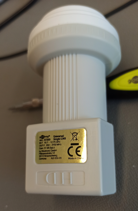
Unmodified Goobay 67269 LNB
The LO signal of the LNB is referenced to a 25 MHz crystal. In low-band operation, the 25 MHz is multiplied by a factor of 390, in high-band operation the multiplication factor is 424. While a standard 25 MHz crystal reference is stable enough for broadband satellite TV reception, it is insufficient for the reception of narrow-band signals commonly found on radiocommunication satellites such as the popular, geostationary QO-100 (Qatar Es’hail 2). Therefore, the desire arises to lock the LO to an externally provided reference.
This also opens up the possibility to change the LO-frequency so that the IF-frequency range can be moved to a more convenient range. For instance, the narrow-band transponder of QO-100 has a downlink frequency range of 10489.5 to 10490 MHz. The standard LO-frequency of 9750 MHz results in an intermediate frequency (IF) frequency range of 739.5 to 740 MHz. If the reference frequency is changed to 25.780 – corresponding to a LO-frequency of 10054.20 MHz -, the resulting IF frequency range would move to 435.30 MHz – 435.80 MHz, right in the center of the 70 cm amateur radio band.
Modification
The modification itself is quite simple. In essence, the 25 MHz crystal is removed and replaced by a 25 MHz LC-series resonant circuit with bandpass characteristic connected to the F-connector of the LNB. Standard component values of 18 pF and 2,2 µH were chosen for the series LC circuit.
(1) 
This in an impedance of 8.1 Ω at a frequency of 25 MHz. At 26 MHz the resulting impedance is 19.32 Ω, at 27 MHz this value further increases to 45.74 Ω (Eq. 1).
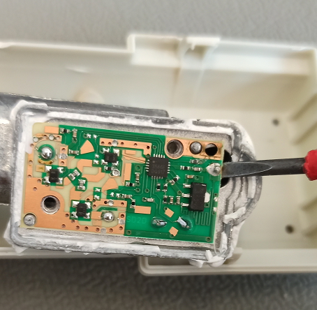
After removing the plastic cover using a flat screwdriver, the metal cover for the PCB housing can be removed after loosening two screws. The required screwdriver is of type Torx T8. After removal of the metal cover, the top-side of the LNB’s PCB is accessible.
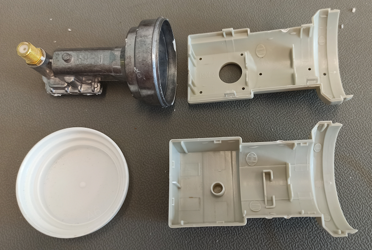
Plastic cover of the LNB removed
Removal of the PCB housing screws
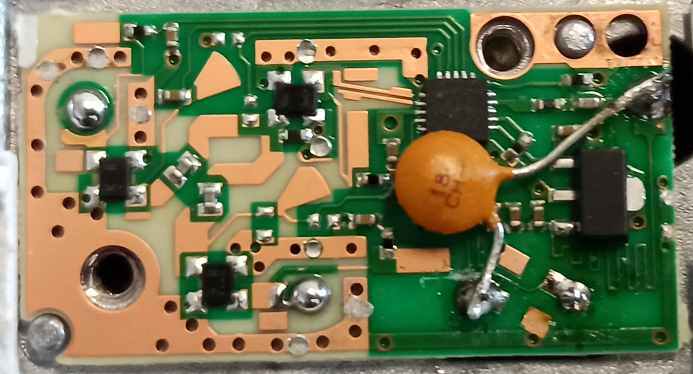
The main function blocks of the LNB’s PCB can easily be identified. The circuit design is centered around a fully integrated PLL/LO/Downconverter-chip marked “3566E”. Even after a thorough search, very little information on this chip can be found. However, knowing the general working principle of such a chip, the relevant parts of the circuit can be reverse engineered without specific device information at hand.
The DC supply-voltage from the F-connector is passed to a 7806-type voltage regulator through a printed circuit board inductor (yellow rectangle), supplying the 3566E with stable 6 V DC. The PINS marked XTAL1 and XTAL2 connect to a 25 MHz crystal located on the backside of the PCB.
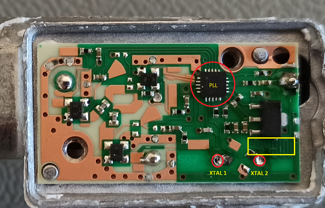
Closeup of the PCB with markings for the PLL, crystal pins and the printed circuit board inductor choke in front of the voltage regulator (yellow rectangle)
In order to identify the proper input pin for injection of an external LO-reference-signal, the waveforms on pin 1 and pin 2 where examined using an oscilloscope. Pin 2 of the 3566E (XTAL2) was consequently identified to be the most suitable pin for injection of an external reference signal.
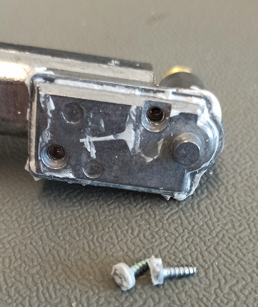
After removal of a single solder pin right above the F-connector, the PCB can be removed from the casing. It was found to be best to apply a slight upward pressure to the PCB while heating the solder joint.
Applying slight upward pressure right next to the solder-joint
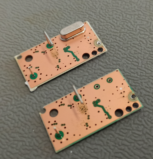
Two of the LNB PCBs before the modification (top) and after the removal of the 25 MHz crystal (bottom)
The 25 MHz, through-hole crystal on the back of the PCB was removed using a soldering iron and solder wick. A 2.2 µH inductor was then installed instead of the previously removed crystal. In order to protect the leads of the inductor from unintended contact with the grounded enclosure, it was covered with a small piece of Kapton tape. The PCB was then re-installed inside the metal enclosure and soldered back in place.
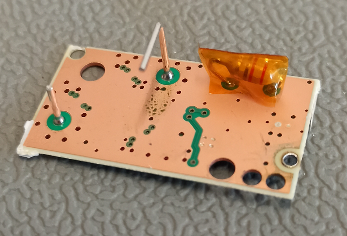
2.2 µH inductor installed in lieu of the removed 25 MHz crystal
The now unnecessary and hindering PCB trace connecting the crystal socket pin previously described as “XTAL 1” and the 3566E PLL was cut using a sharp object. Lastly, the 18 pF capacitor has been soldered between the input connection pin (from the F-connector) and XTAL 1.
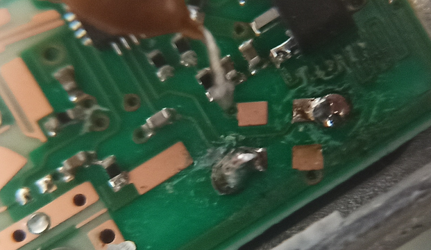
The PCB-trace connected to pin XTAL 1 has been cut using a sharp tool
A 18 pF capacitor has been installed between the F-connector input pin and the XTAL 1 pin, connecting directly to the 2.2 µH inductor
Test and Results
In order to test the functionality of the performed modification, the LNB was connected to a makeshift diplexer with integrated bias tee. Absolutely no care was taken to match the LNB’s input impedance of 75 Ω to the 50 Ω impedance of the equipment used in this test.
The high-pass path of the diplexer (fc = 100 MHz) was connected to a RTL2832 SDR through a 10 dB attenuator. The low-pass path of the diplexer (fc = 30 MHz) was connected to a signal generator. The signal generator was then set to a frequency of 25.78 MHz, resulting in a LO-frequency of 10054.2 MHz if locked on correctly. 14 VDC were then supplied to the LNB through the bias tee of the diplexer. It was observed that the LNB draws a current of 60 mA when unlocked. This value jumps to approx. 90 mA when the PLL has properly locked onto the external reference signal. Lock was observed at a signal amplitude of 3 Vpp into the diplexer. At 75 Ohms, this corresponds to a drive level of around 12 dBm.
Two signals of 3496 MHz and $3496.333 MHz were generated using an ADF4351 evaluation board from Analog Devices. The third harmonics of said signals should produce suitable test signals with frequencies of 10.488 GHz and 10.489 GHz. The ADF4351 evaluation board was set to hop between both frequencies at a rate of 500 ms.
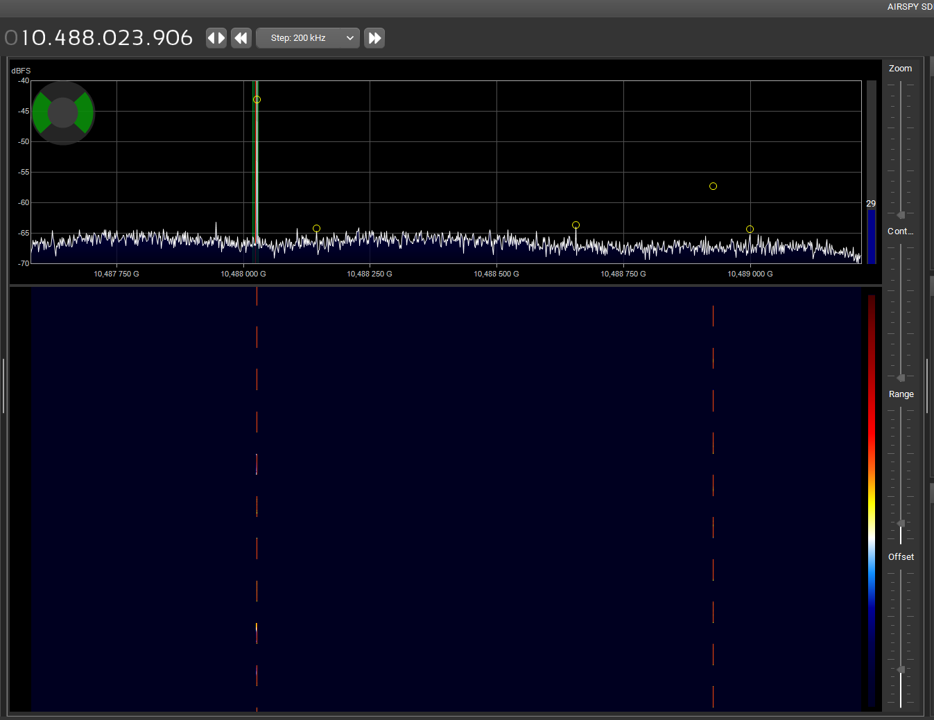
LNB signal output viewed in SDRSharp
The resulting output spectrum was viewed in AirSpy SDR# Studio. The two test signals were clearly visible and the alternating 500 ms hops confirmed their identity. It was noted that due to the high gain of the LNB, it was very easy to overdrive the LNB. Despite using the third harmonic of signals with an amplitude of -4 dBm, the LNB had to be pointed away from the signal source in order not to cause distortion. Further, the 10 dB attenuator in front of the RTL2832 SDR was absolutely necessary in order not to exceed the full-scale dynamic range of the receiver.
It was further observed that varying the frequency of the reference signal between 24 MHz and 27 MHz does indeed change the LO-frequency without a visible change in IF output power or spurious frequency components.
Conclusions
This article shows that it is possible to successfully modify an inexpensive Goobay 67269 LNB to accept an external reference signal. Furthermore, the experiments shown demonstrate that the LNB is capable of down-converting K-band signals outside of the manufacturer’s specified frequency range.
Links and Sources:
[1] Westerhold, S. and Matlinski, C., “Modification of a Goobay 67269 LNB for use in 10 GHz communication satellite reception”, Jul. 2023, doi: 10.5281/zenodo.8102235.
[2] Armin Duft. “Goobay 67269 LNB Modification”. In: (2019). url: https://dh1da.darc.de/projekte/Amateurfunk/QO-100_LNB/Goobay_67269_LNB_Mod-DH1DA.pdf (visited on 07/01/2023).
[3] Wentronic GmbH. Universal Single LNB | Wentronic. url: https://www.wentronic.com/de/universal-single-lnb-67269 (visited on 07/01/2023).
Westerhold, S. (2023), "LNB Modification for 10 GHz QO-100 Satellite Reception". Baltic Lab High Frequency Projects Blog. ISSN (Online): 2751-8140., https://baltic-lab.com/2023/07/lnb-modification-for-10-ghz-qo-100-satellite-reception/, (accessed: July 28, 2026).

- Conducted Emissions on the Bench: Implementing the CISPR 25 Voltage Method - December 15, 2025
- WebP-Images without Plugin - January 14, 2025
- Firewall Rules with (dynamic) DNS Hostname - January 14, 2025
Teukka
A thought that occurred to me as I read about this on HaD was that this method has more applications than tweaking the LO for QO-100, which is to feed a reference to LNB’s when you need more stability and precision when listening to satellites in the microwave band (i.e. having a good standard in your shack which you feed to the LNB(s)).
A question is how much space do you have inside the LNB? A generic PCB with a similar form factor as the crystal (maybe with tweaks to allow for different sockets/pinouts) could be an idea.
Another question I have is how common is 25 MHz as the reference in LNB’s?
Sebastian
There’s little to no space inside the LNBs. The space previously occupied by the crystal is really the most one can work with. But I intend to try exactly what you suggested; Implement a small PCB that fits in the crystal location and houses a TCXO. One work-around to get more room to play is to use so called “Twin” or “Dual” LNBs. They basically house two LNBs in one housing and thus offer more room. Plus they actually offer two F-connectors. So one could disconnect one section and use the now available F-connector as convenient location to connect an external clock-source. 25 MHz is pretty much the standard. So are the multiplication factors mentioned in the article. Common Mixer-/Pll-/LO-chips are the RDA3560M, RDA3566, TFF1015HN and TFF1017HN. They’re all very similar. Unfortunately, I haven’t found a reliable source of these chips. Else I might even consider completely designing a drop-in PCB for amateur radio use.
Ali
I tried this mod on a very similar LNB, and got similar results up to the point where I can see a rise in current consumption when I connect the reference signal, but I can’t see my test signal (also 3rd harmonic of which I generate with a pluto). I verified that the test signal is visible with an unmodified LNB, but with a modified one, all I see is the noise floor rising, so the LNB is obviously doing something, I just can´t tell what, exactly.I played with a lot of different signal levels for the reference signal without much success. I even tried another LNB with the same result. Have you observed something similar during your tests, and are you able to point me in the right direction?