UPDATE: There also is a German version of this article available on my German blog: Arduino GIGA R1 WiFi | Audio Loopback Beispiel-Code
General Overview
The new Arduino GIGA R1 WiFi offers great potential as an inexpensive platform for DSP audio experiments. Elektor kindly sent me a review sample of the Giga R1 [1]. With 12 ADCs, features two 12-bit buffered DACs and plenty of memory and horsepower, it was only logical to see how well the Giga performs in the world of DSP. The obvious starting point is to implement an audio-loopback-device. Since I was unable to locate any working code examples, I quickly cooked up a sketch from scratch using the Advanced Analog Library.
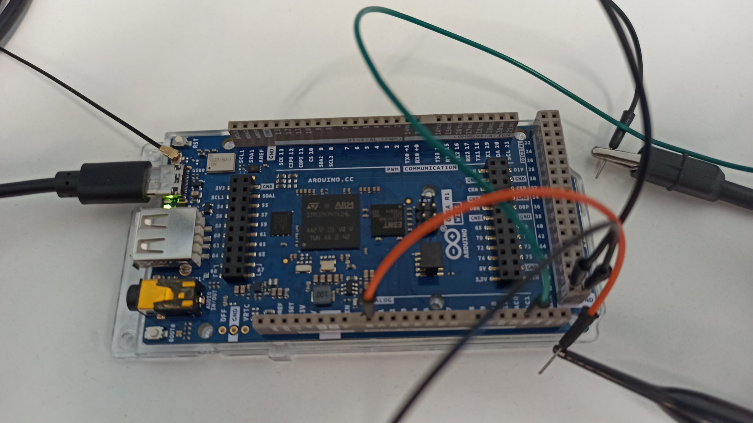
Arduino GIGA R1 WiFi being evaluated as an audio DSP platform
Arduino Code
/** Arduino Giga R1 WiFi - Audio Loopback Example** Copyright (C) 2022 Westerhold, S. (AI5GW)* ORCID: https://orcid.org/0000-0001-7965-3140* Web (EN): https://baltic-lab.com** This program is free software: you can redistribute it and/or modify* it under the terms of the GNU General Public License as published by* the Free Software Foundation, either version 3 of the License, or* (at your option) any later version.*/#include <Arduino_AdvancedAnalog.h>// Instantiate ADC 0 (Pin A0) and DAC 0 (Pin A12)AdvancedADC ADC0(A0);AdvancedDAC DAC0(A12);void setup() {Serial.begin(9600);// Set-up ADC0, stop program on failure// Resolution, sample rate, number of samples per channel, queue depth.if (!ADC0.begin(AN_RESOLUTION_12, 44100, 128, 128)) {Serial.println("ADC fail...");while (1);}// Set-up DAC0, stop program on failure// Resolution, sample rate, number of samples per channel, queue depth.if (!DAC0.begin(AN_RESOLUTION_12, 44100, 128, 128)) {Serial.println("Failed to initialize DAC 1");while (1);}}void loop() {if (ADC0.available()) {// Get handle for the input bufferSampleBuffer inBuf = ADC0.read();// Get handle for the output bufferSampleBuffer outBuf = DAC0.dequeue();for (int i = 0; i < inBuf.size(); i++) {// Copy contents of input buffer to the output bufferoutBuf.data()[i] = inBuf[i];}// Write contents of the output buffer to the DACDAC0.write(outBuf);// Release the input bufferinBuf.release();}}
Test Results
After compiling the code and flashing the Arduino GIGA R1 WiFi, a signal generator was connected to the A0 input pin. The DAC0 output pin was monitored using an oscilloscope. The first test was performed by applying a 800 Hz sine wave signal with an amplitude of 1 Vpp and an offset-voltage of 500 mV. The offset voltage is necessary because the DACs of the Arduino Giga R1 WiFi are not capable of generating negative voltages.
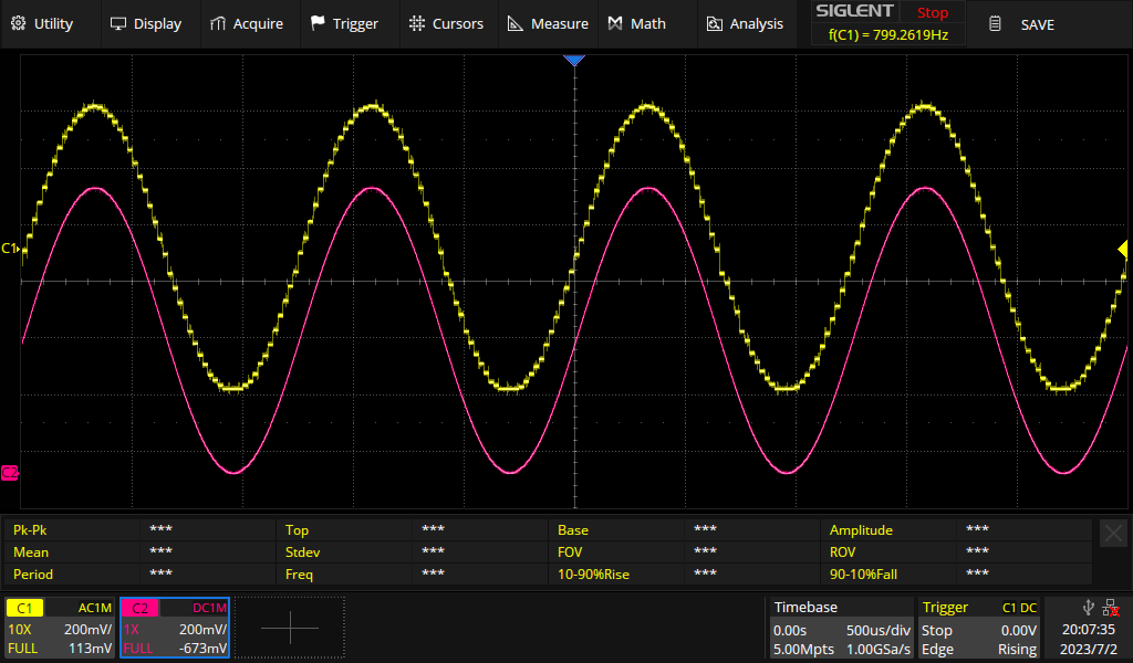
800 Hz sine-wave (bottom trace) fed into the Arduino Giga R1 WiFi (bottom), Output on pin DAC0 from the Arduino (top trace)
A more close-up view reveals the typical stair-steps of the DAC. For actual audio applications, the output signal would obviously have to be filtered. Note that absolutely no care was taken to adjust the conversion frequency of the DAC in any way. The examples were implemented using the default configurations.
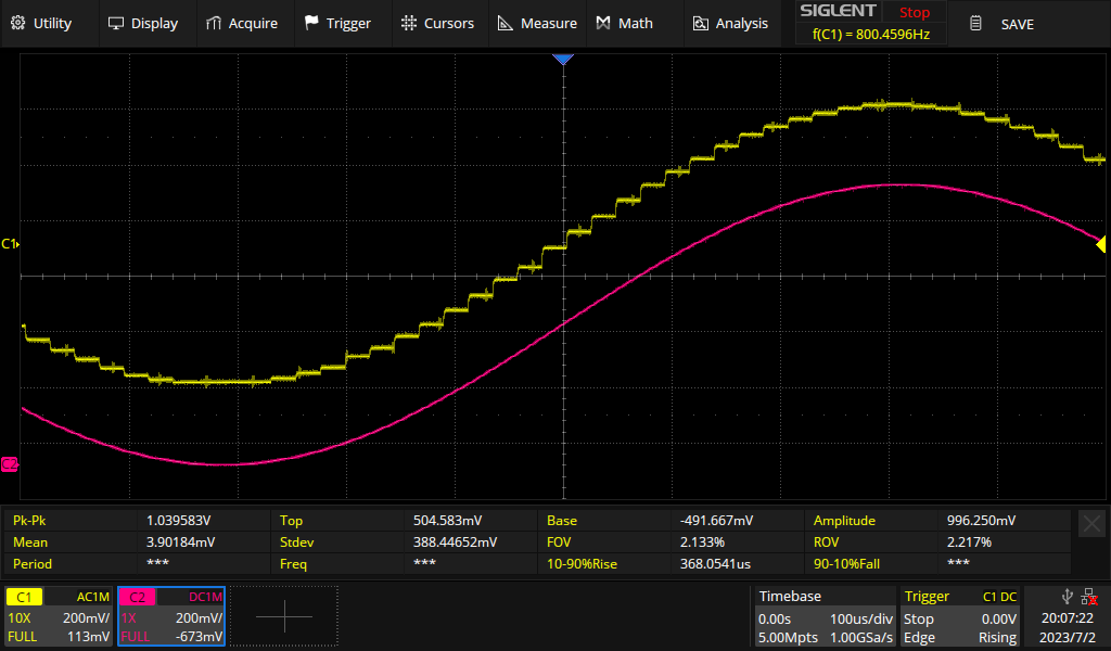
Closeup of the same 800 Hz sine wave shown in the previous picture
Next, the waveform was changed to a 1 kHz square wave. The amplitude settings were left unchanged.
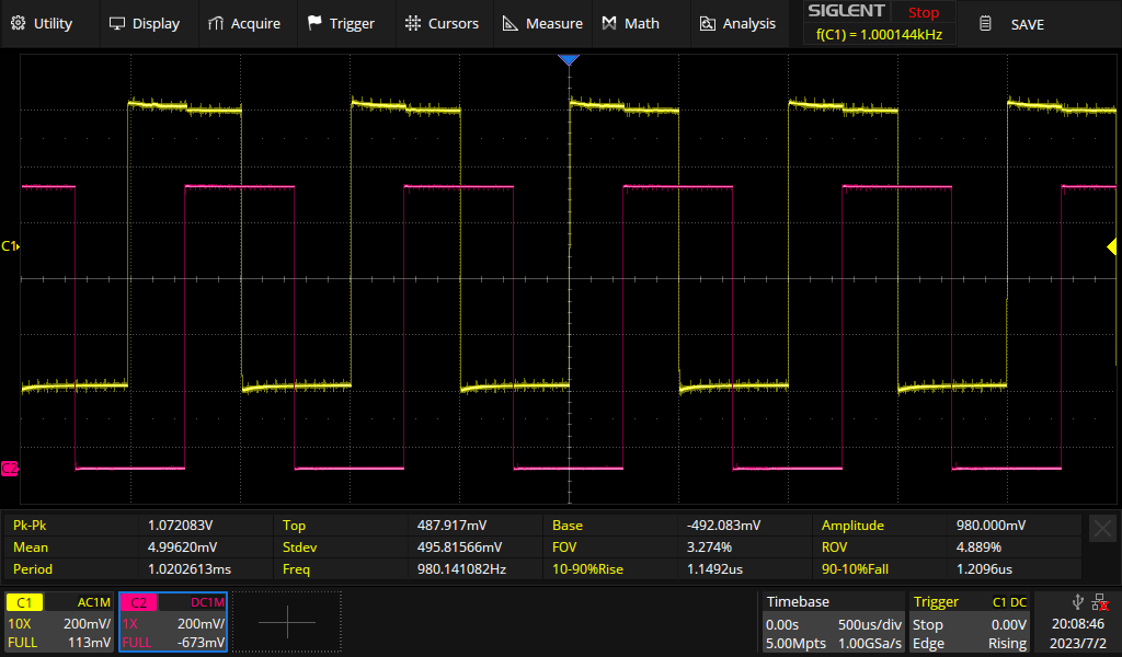
1 kHz square wave test. Bottom trace; Input, Top Trace: Output from DAC0
Lastly, a ramp signal with a frequency of 1 kHz and an amplitude of 1 Vpp and an offset-voltage of 500 mV was applied to the A0 input.
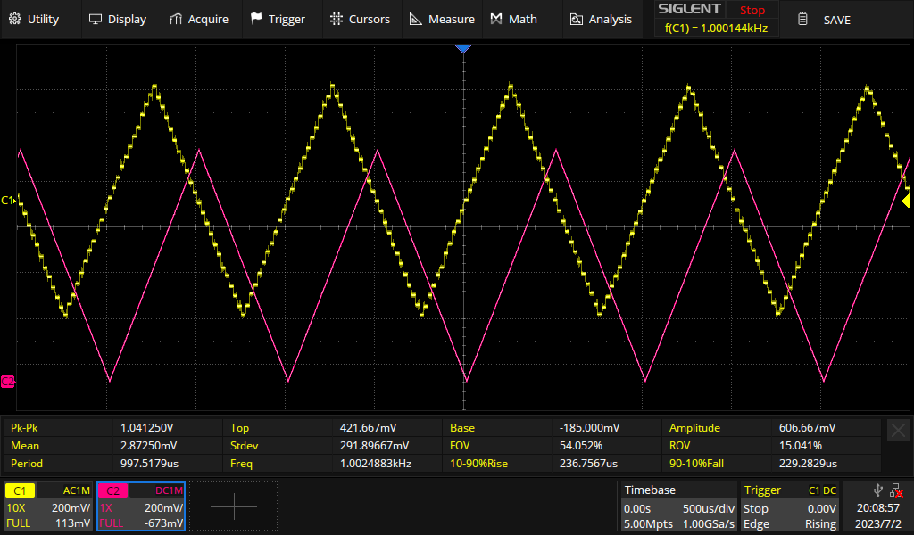
1 kHz ramp signal test. Bottom trace; Input, Top Trace: Output from DAC0
Conclusion
The sketch provided above provides a great starting point for audio DSP experiments. Instead of simply copying the input buffer straight to the output buffer, it would be quite easy to manipulate the input buffer to achieve certain DSP-functions.
Links and Sources:
[1] Arduino Giga R1 WiFi, Elektorstore: https://www.elektor.com/arduino-giga-r1-wifi
Westerhold, S. (2023), "Arduino GIGA R1 WiFi | Audio Loopback Example". Baltic Lab High Frequency Projects Blog. ISSN (Online): 2751-8140., https://baltic-lab.com/2023/07/arduino-giga-r1-wifi-audio-loopback-example/, (accessed: June 4, 2026).

- Conducted Emissions on the Bench: Implementing the CISPR 25 Voltage Method - December 15, 2025
- WebP-Images without Plugin - January 14, 2025
- Firewall Rules with (dynamic) DNS Hostname - January 14, 2025