General Overview
The most common reference signal frequency in professional labs is 10 MHz. Many GPS disciplined frequency standards, therefore, provide 10 MHz signals and most professonal laboratory equipment has 10 MHz reference input connectors. When it comes to a QO-100 satellite station, one might need a 25 MHz reference signal for the LNB, a 40 MHz reference signal for the ADALM Pluto and the transmit transverter usually requieres yet another, different reference frequency. While some GPSDOs, such as the common Leo Bodnar devices, have the ability to change the output clock frequency, it still doesn’t solve the problem of generating multiple clock reference signals with different frequencies. The ICS501 / ICS502 devices might appear like a good (but obsolete) part for frequency translation. However, their phase noise performance is subpar. While researching, I came across the VersaClock 6E devices from Renesas.
The devices I tried are the 5P49V6965 and 5P49V6975. Both devices are capable of providing 4 independent outputs with frequencies ranging from 1 kHz to 350 MHz with a low phase noise PLL of typically les sthan 0.5ps RMS phase jitter. Two different reference clock inputs provide additional flexibility. The first input is designed to support an external crystal as frequency selective device with a crystal frequency range from 8 to 40 MHz. A second, external clock input accepts reference signals from 1 to 200 MHz in single-ended mode [1,2].
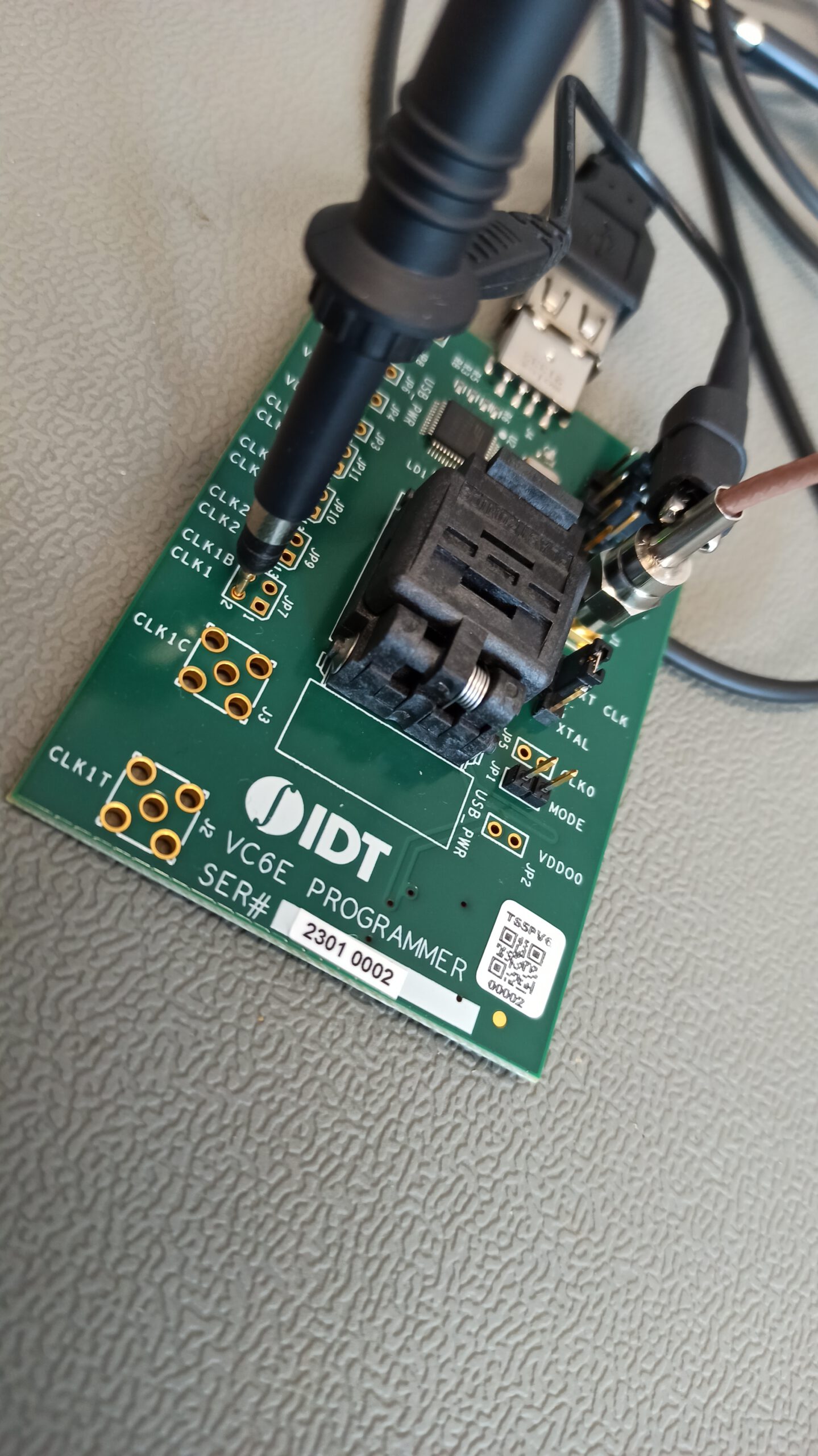
Programming Kit for VersaClock 6E devices, such as the 5P49V6965 and 5P49V6975
Using the Programming Kit for VersaClock 6E [3] and the software IDT Timing Commander, a 5P49V6965 was programmed to generate 3 different output signals with frequencies of 25 MHz, 40 MHz and 100 MHz from an external 10 MHz reference signal.
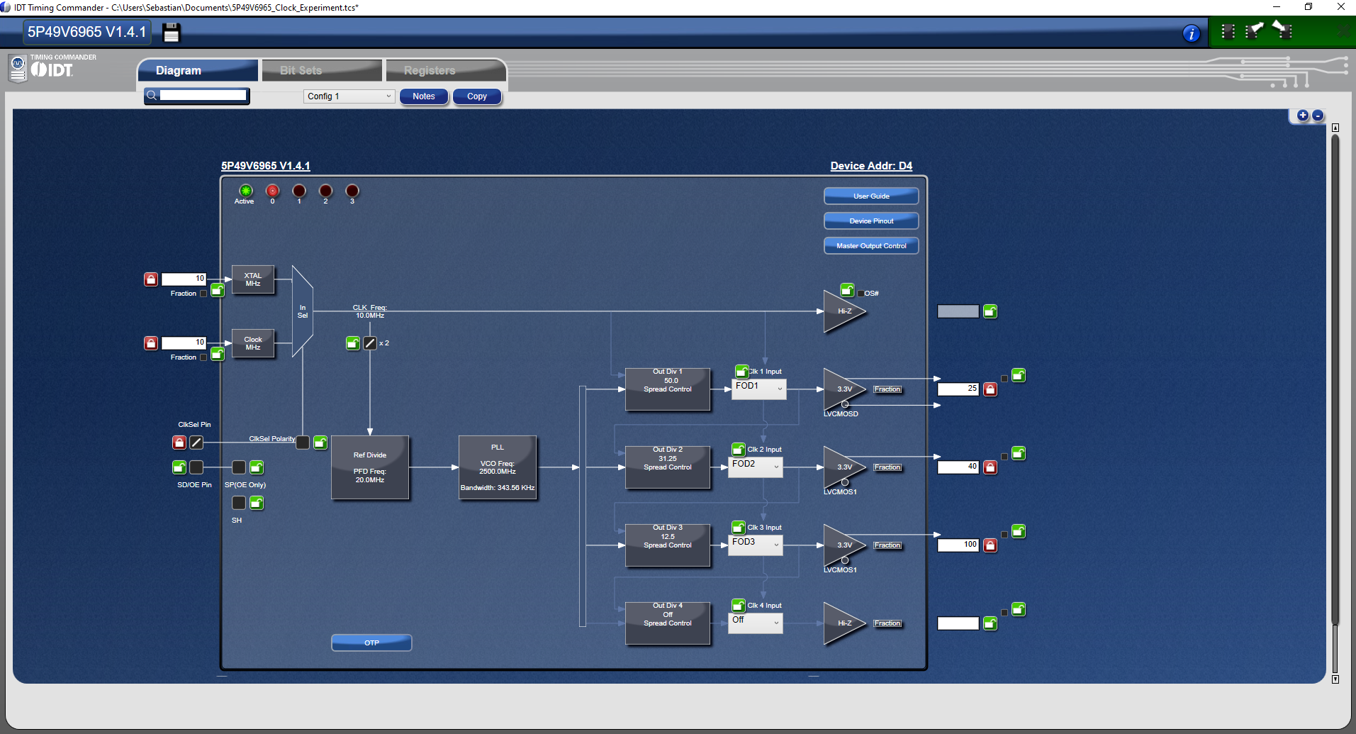
IDT Timing Commander used for testing and programming the 5P49V6965 and 5P49V6975
After writing the desired values to the 5P49V6965, an external 10 MHz reference signal was connected to the board and the output was ovserved using an oscilloscope. It should be mentioned that absolutely no care was taken to implement proper impedance matching.
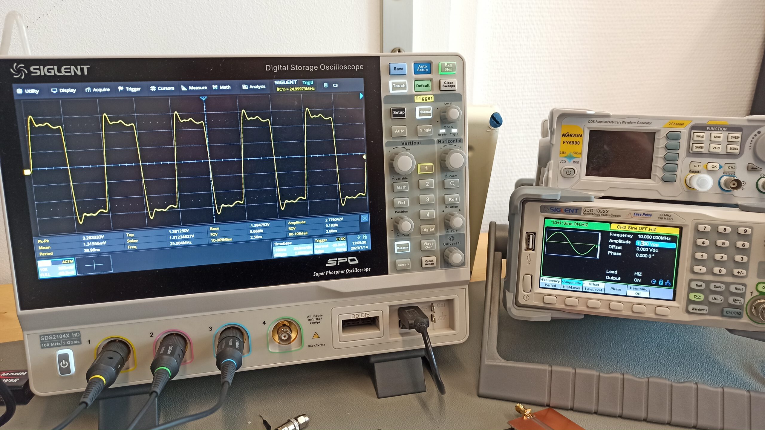
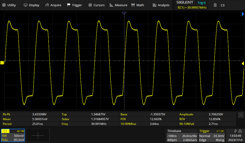
Example output of a 25 MHz signal from a 10 MHz reference signal by a Renesas 5P49V6965
Test Results
The first thing that was observed, was that the 5P49V6965 has absolutely no problem accepting external, sinusoidal reference signal with negative amplitude components. When the reference generator’s output amplitude was set to 1 Vpp with no offset, thus sending the negative half-wave down to -500 mV, the device locked onto the reference signal perfectly. When a square wave is used, the necessary minimum signal amplitude for a proper lock was even lower.
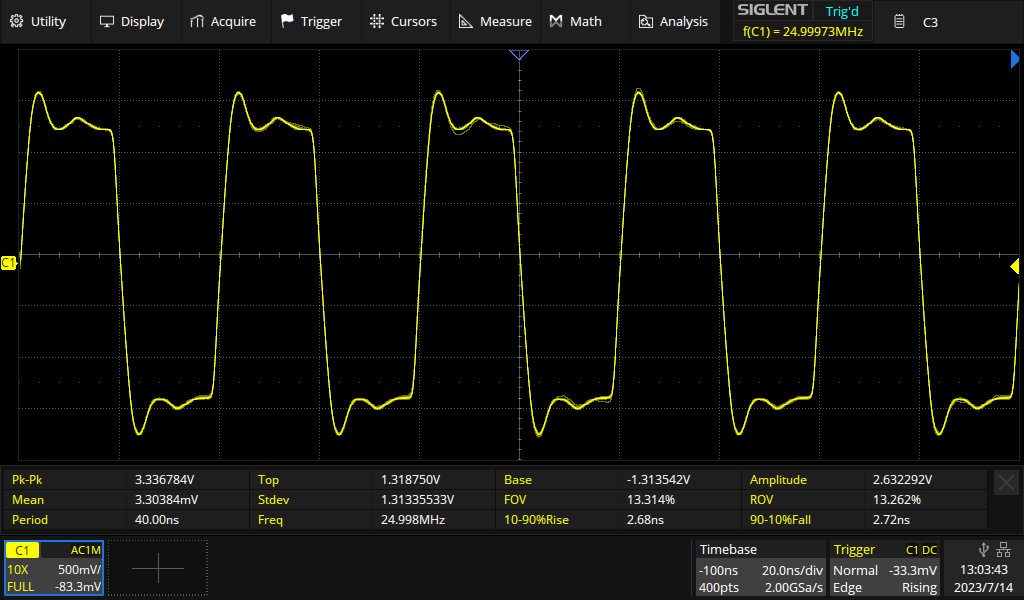
25 MHz clock signal generated from an external 10 MHz reference signal by a 5P49V6965
40 MHz clock signal generated from an external 10 MHz reference signal by a 5P49V6965
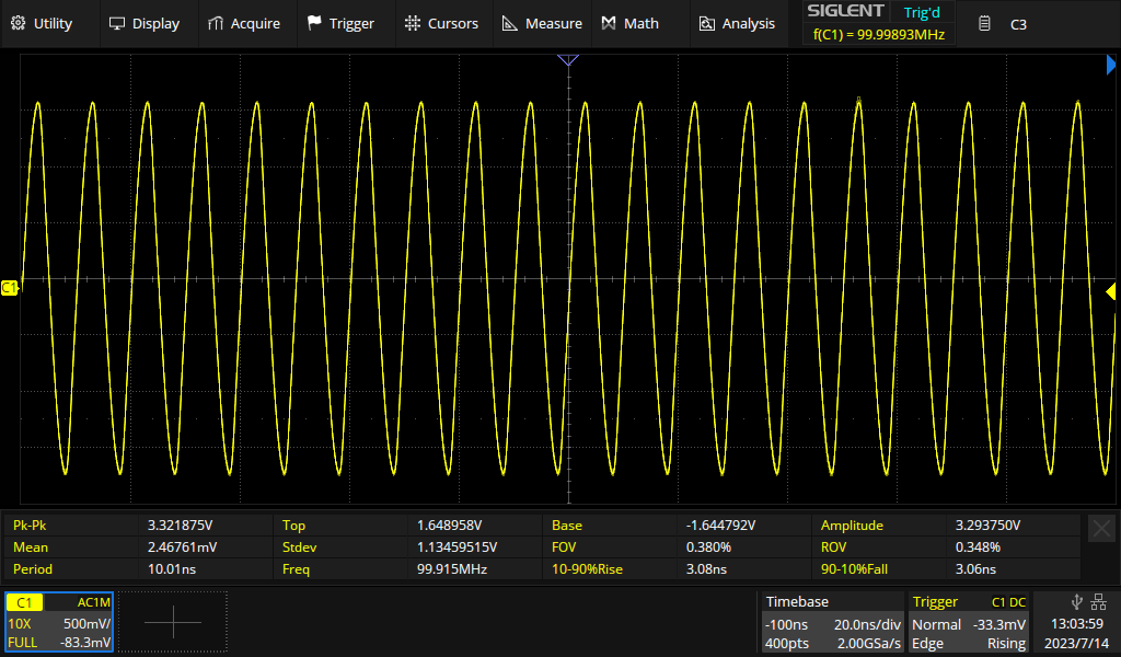
100 MHz clock signal generated from an external 10 MHz reference signal by a 5P49V6965
Unsurprisingly, the outputs generated signals of 25, 40 and 100 MHz according to their programming.
Conclusions
The 5P49V6965 and 5P49V6975 devices appear to be perfect candidates for a univeral clock translator board that can be programmed to provide 4 different reference frequencies from a single, standard reference clock source. The next step is to design a prototype PCB that properly takes care of input- and output termination to a systems impedance of 50 Ohms. The two different clock inputs of the device and the clock select pin open up an easy implementation of an on-board TCXO with automatic switchover when an external reference is applied to the PCB. Since 4 different, hardware selectable configurations can be burned into the device, the most commonly needed reference frequency can be programmed into the device and be selected by jumpers.
Links and Sources:
[1] 5P49V6975 Datasheet, Renesas: https://www.renesas.com/us/en/document/dst/5p49v6965-datasheet?language=undefined
[2] 5P49V6965 Datasheet, Renesas: https://www.renesas.com/us/en/document/dst/5p49v6975-datasheet
[3] Programming Kit for VersaClock 6E, Renesas: https://www.renesas.com/us/en/products/clocks-timing/clock-generation/programmable-clocks/5p49v6965-prog-programming-kit-versaclock-6e
Westerhold, S. (2023), "Universal Clock Translator using Renesas VersaClock 6E Devices". Baltic Lab High Frequency Projects Blog. ISSN (Online): 2751-8140., https://baltic-lab.com/2023/07/universal-clock-translator-using-renesas-versaclock-6e-devices/, (accessed: June 23, 2026).

- Conducted Emissions on the Bench: Implementing the CISPR 25 Voltage Method - December 15, 2025
- WebP-Images without Plugin - January 14, 2025
- Firewall Rules with (dynamic) DNS Hostname - January 14, 2025