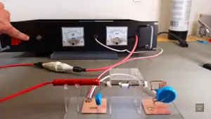
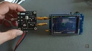
Conducted Emissions on the Bench: Implementing the CISPR 25 Voltage Method
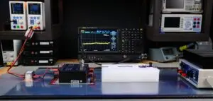
This article pulls back the curtain on CISPR 25 conducted-emissions testing, demonstrating how a fully functional voltage-method setup can be built and operated on a standard lab bench. This approach shows how conducted emissions can be characterized with precision using accessible tools and a carefully structured setup, while walking through all critical elements needed to … [Read more…]