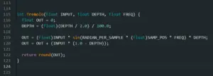
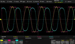
Critical length of a PCB trace and when to treat it as a transmission line

Ideally, the impedance of PCB traces should be matched to the load and source impedances. This becomes especially important in high-frequency and high-speed digital PCB designs. Various rules of thumb are available to determine the critical length at which a PCB trace should be treated as a transmission line. Below this critical length, an impedance mismatch can safely be ignored. Or can it?

SAW filter PCB with SMA connectors for 1090 MHz (ADS-B). Mismatched input and output traces (Z=100 Ohms, l=3,5mm) have been deemed acceptable.

SAW filter PCB with SMA connectors for 1090 MHz (ADS-B). Mismatched input and output traces (Z=100 Ohms, l=3,5mm) have been deemed acceptable.

Rule of Thumb

Rules of thumb are made to simplify our everday engineering life. For the critical length of a PCB trace, there are various different rules of thumb available. One of those rules is the 1/10 rule (Eq. 1). It basically states that the critical length for a PCB trace is 1/10th of the wavelength. It suggests that for length smaller than 1/10 of a wavelength, any impedance (mis)match and transmission line effects can safely be ignored.

(1)   \begin{equation*}  l_{crit} = \frac{\lambda}{10 \sqrt(\varepsilon_r)} \end{equation*}

The \varepsilon _r term in the equation corrects for the difference between physical length and electrical length. \varepsilon _r is equal to the relative permittivity, also oftentimes called the dielectric constant (Dk), of the PCB material used. For FR4 this varies between about 4.3 and 4.5. \lambda is of course the wavelength as defined by the speed of light divided by the frequency.

When working with digital singals, the critical length is expressed as a function of the rise or fall time(Eq. 2).

(2)   \begin{equation*}  l_{crit} = \frac{0.25 t c_0}{\sqrt(\varepsilon_r)} \end{equation*}

Where t denotes the rise- or fall-time (whichever is smaller) and c_0 the speed of light.

Now that we have commonly accepted rules of thumb and can easily calculate the length of a PCB trace below which we can safely ignore pesky things such as impedance matching and the relative permittivity of the PCB material used, I could wrap up this article and just leave it at that, right? Unfortunately, no…

What exact fraction of a wavelength to consider to be the threshold for the critical PCB-trace length varies by literature and people’s personal preferences. There’s also the 1/4, 1/8, 1/16 and 1/20 rule and many more. So which one of these is correct and which one should you use?

Transmission Line Math

To the question of when a PCB trace should be regarded as a transmission line, the short answer is: Always! To answer the question of when it really matters, we will have to dive a little bit into the science involved. Equation 2 shows the complex input impedance (Z_{IN}) of any stripline of length l in metres. Z_0 is the characteristic impedance of the transmission line itself, in this case the PCB trace. \beta is the propagation constant with the peculiar unit of radians per metre (Eq. 4). Z_L denotes the load impedance present at the end of the transmission line.

(3)   \begin{equation*}  Z_{IN} = Z_0 \frac{Z_L + j Z_0 tan(\beta l)}{Z_0 + j Z_L tan(\beta l)} \end{equation*}

(4)   \begin{equation*}  \beta = \frac{2 \pi}{\lambda} = \frac{2 \pi f}{c_0} \end{equation*}

The abomination of an equation can be simplified very slightly if the length l is given as a factor relative to the wavelength, for instance 0.25 or 1/4 for a quarter wavelength (Eq. 5).

(5)   \begin{equation*}  Z_{IN} = Z_0 \frac{Z_L + j Z_0 tan(2 \pi l)}{Z_0 + j Z_L tan(2 \pi l)} \end{equation*}

From this equation it is apparent that there is only a single case where the length of the PCB trace doesn’t matter. And that is when Z_0 = Z_0. Or in other words when the trace impedance perfectly matches the load impedance, for instance 50 Ohms. Under any other condition, except at length 0 (and multiples of 1/2 wavelength), the trace impedance will have some influence on the impedance seen at the beginning of the trace. But by how much and how much is acceptable?

A picture is worth a thousand words as they say. Let’s assume a load impedance of 50 Ohms and arbitrarily pick mismatched trace impedances of 60, 70, 80 and 90 Ohms. Using equation 4, the impedance seen at the beginning of the trace can be plottet as a function of electrical length.

Input impedance as a function of electrical length and trace-impedance.

Input impedance as a function of electrical length and trace-impedance.

Just for fun, I also plottet the same function with trace impedances of 20, 35, 65 and 80 Ohms. However, a smaller characteristic impedance of a PCB trace means that it is too wide. In that instance, honestly, just make it thinner and match it to 50 Ohms. Because the usual case of why we even might want to ignore impedance matched traces is because of their width. Especially in home made projects or when using one’s favorite chinese PCB manufaturer, the default PCB material is 1.6mm thick FR4. Assuming a dielectric constant of roughly 4.3, a microstripline with a characteristic impedance of 50 Ohms would have a thickness of around 3.1 mm. Using just 1mm thick FR4 with the same dielectric constant would reduce this to a more acceptable 2mm. Additionally, FR4 has the tendency to not have a very well controlled dielectric constant.

Input impedance as a function of electrical length and trace-impedance.

Input impedance as a function of electrical length and trace-impedance.

The previous graphs confirm what the math already showed: Any length (except 0) of a mismatched PCB trace has an influence on the input impedance of the trace. To decide what is acceptable and what not, we have to define what we will accept in our designs. Two possible figures of merit vould be the VSWR or the mismatch loss. The mismatch loss indicates how much of the input power is lost due to the impedance mismatch. I included two horizontal lines enclosing a VSWR of < 1:1.1, which corresponds to a mismatch loss of 0.01 dB. Another pair of horizontal lines marks the area in which the mismatch loss is below 0.1 dB, corresponding to a VSWR 1:1.356. At a VSWR of 1:1.356, 97.72 % of the transmitted power reaches the load, 2.28 % get reflected back to the load. At a VSWR of 1:1.1, these values improve to 99.77 % forward power and 0.23 % reflected power.

Input impedance plottet as a function of trace impedance for trace lengths of 1/10, 1/16 and 1/20 of a wavelength.

Input impedance plottet as a function of trace impedance for trace lengths of 1/10, 1/16 and 1/20 of a wavelength.

What you deem acceptable for your design is entirely up to you. Personally, in my hobby designs I yield for a mismatch loss of less than 0.1 dB. As shown in the graph, using the 1/10 rule of thumb will quickly put the design outside of those limits. The 1/16 rule (Eq. 6), however, is a really good and useful approximation. At least for PCB traces with a characteristic impedance of less than 110 Ohms. By simply keeping all relevant traces wider than 0.75 mm (max. Z ~100 Ohms, FR4, Dk=4.3, PCB thickness=1.6mm) I effectively eradicate the need to double check the trace impedance in addition to the critical length.

(6)   \begin{equation*}  l_{crit} = \frac{\lambda}{16 \sqrt(\varepsilon_r)} \end{equation*}

The periodicity of the input impedance at 1/2 wavelength intervals is also an interesting phenomenon. Half a wavelength corresponds to 180 degrees of phase shift. For a reflected signal the total round trip delay would thus be 360 degrees. Assuming a periodic signal, the reflected signal would thus be in phase with the “new” signal at the input. Therefore, one could theoretically intentionally design a mismatched transmission line with a total length less than the critical length plus any integer multiple of 1/2 \lambda.

Periodicity of the input impedance of a mismatched transmission line as a function of electrical length

Periodicity of the input impedance of a mismatched transmission line as a function of electrical length

Conclusions

Within certain constraints, rules of thumb can be an effective guide to estimate the critical length of a PCB trace. However, it is important to be aware of one’s own design requirements and not be tempted to completely ignore any transmission line effects regardless of length.


Etching PCBs using hydrochloric acid and hydrogen peroxide

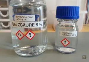
Choosing the right etchant for home made PCBs could be a science on its own. Some people prefer ferric chloride, some advocate for sodium persulfate and I personally prefer hydrochloric acid and hydrogen peroxide. This article shows how to use a mixture of hydrochloric acid and hydrogen peroxide in a safe and controllable manner.

UPDATE: There also is a German version of this article available on my German blog: Leiterplatten mit Salzsäure und Wasserstoffperoxid ätzen

Introduction

Using a combination of hydrochloric acid (HCl) and hydrogen peroxide H2O2 in itself is nothing new. When I recently rediscovered this method (because I was out of sodium persulfate), I was amazed by the quality and sharpness of the resulting traces and pads. I shared my amazement on Twitter [1]. To my surprise, the responses were extremely divided. Many people confirmed that they have been using the same etchant for a long time and had great success with it. Others proclaimed it was a terrible etchant, extremely dangerous and poor controllability. As always, the devil is in the details. The group confirming the high reliability of hydrochloric acid and hydrogen peroxide as an etchant use – just like me – highly diluted solutions. Just like the common saying “it is the dose that makes the poison” goes, for use as an etchant it is absolutely essential to use proper concentration levels.

Etchant Preparation

For 1 litre of etchant the following ingredients are used:

  • 700 ml distilled water
  • 200 ml 30-35 % hydrochloric acid (HCl)
  • 100 ml 12 % Hydrogen Peroxide (H2O2)

All ingredients are added together in a beaker. Water is added first, then the hydrochloric acid, lastly the hydrogen peroxide.

Two GL45 bottles containing 8 % hydrochloric acid (left) and 12 % hydrogen peroxide (right)

Two GL45 bottles containing 8 % hydrochloric acid (left) and 12 % hydrogen peroxide (right)

Concentrated hydrochloric acid, also called muriatic acid, does fume a lot and the fumes are quite unpleasant to breathe in. The fumes are also highly corrosive to anything near it. So in order to mitigate the possible hazards, and to simplify the preparation of the etching solution, I prepared an 8 % hydrochloric acid solution in a well ventilated area. Additionally, I prepared a 12 % hydrogen peroxide solution. Both are safe for storage and use in a regular indoor lab. The concentrations were chosen to further simplify the preparation of the etchant: 9 parts of the 8 % HCl and 1 part of the 12 % H2O2 solution are added together to yield 10 parts of ready to use etchant solution. For example, adding 90 ml of the 8 % HCl and 10 ml of the 12 % H2O2 solution yield 100 ml of etching solution.

Another option, especially in countries where 12 % hydrogen peroxide is hard to come by, would be to use 3 % H2O2 and premade 14 % hydrochloric acid. In that case, the mixture ratio is further simplified to 1:1. For instance, 500 ml of 14 % HCl and 500 ml of 3 % hydrochloric acid would yield 1 litre of etchant.

It should be noted that hydrogen peroxide likes to decompose when exposed to light. Therefore, the H2O2 stock solution should be kept in an amber glass bottle, or at least be kept away from (natural) light sources.

Hazard of Chlorine gas production

A common warning is, that this method produces extremely dangerous and toxic chlorine gas. While chlorine is always produced (Eq. 1 and 2), it’s release as chlorine gas does depend strongly on the concentration of the HCl and H2O2 used [2]. If the concentrations are kept below a certain threshold, the chlorine is staying in solution and is eventually consumed in another reaction mechanism (Eq. 3).

(1)   \begin{equation*}  H_2O_2 + HCl -> H_2O + HOCl \end{equation*}

(2)   \begin{equation*}  HOCl + HCl -> H_2O + Cl_2 \end{equation*}

(3)   \begin{equation*}  H_2O_2 + Cl_2 -> 2HCl + O_2 \end{equation*}

So how much is too much? To quote directly from a research paper titled “Oxidation of hydrogen chloride with hydrogen peroxide in aqueous solution”:

The oxidation of hydrogen chloride with hydrogen peroxide at common temperature with the evolution of chlorine into the gas phase occurs at a hydrogen chloride concentration in a solution exceeding the threshold value (5.2 M).

A 5.2 M concentration of HCl corresponds roughly to 16.1 %. The concentration used in the etchant recommended in this article is about 2.27 M, less than half of the critical threshold level!

Etching Process

When ready to etch a PCB, I prepare the necessary amount of etchant as describeb before. A glass beaker is used as the container for the etching process. The PCB is completely submersed in the etchant. For a copper thickness of 35 µm (1 oz) the etching time is about 17 minutes at room temperature. After the etching has completed, remove the PCB from the etchant and rinse the PCB with water.

FR4 PCB after 17 minutes in the HCl and H2O2 etchant.

FR4 PCB after 17 minutes in the HCl and H2O2 etchant.

Conclusions

The results are quite satisfactorily. The quality of the traces in regards of sharpness, lack of overetching is outstanding. While standard precautions should be in place when working with chemicals, I can involuntarily state that even a few drops of the etchant won’t eat your flesh anytime soon. Which is no surprise at these high levels of dilution.

Prototype of a Triplexer etched using a hydrochloric acid and hydrogen peroxide etching solution

Prototype of a Triplexer etched using a hydrochloric acid and hydrogen peroxide etching solution

In the beginning of the etching process, the copper is attacked and copper chloride is formed. After a while, the etching process will follow the same chemical principles of using Copper(II) chloride directly [3]. Having a bit of cupric chloride in the etching solution to begin with might help the etching process. In any case, due to it’s regenerative nature, the etching solution should last for a long time. That said, I have never attempted to store used etchant and always prepare a fresh solution when I need it.

YouTube Video

Links and Sources:

[1] Twitter Post, Baltic Lab: https://twitter.com/BalticLabEE/status/1687521760386670592

[2] Oxidation of hydrogen chloride with hydrogen peroxide in aqueous solution, Skudaev, V. and Solomonov, A. and Morozovskii, A. and Isakov, N.: https://link.springer.com/article/10.1134/S1070427208010035

[3] Etching with Air Regenerated Acid Cupric Chloride, By Adam Seychell: http://techref.massmind.org/Techref/pcb/etch/cucl2.htm


Universal Clock Translator using Renesas VersaClock 6E Devices

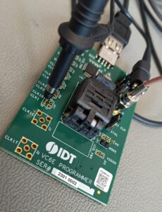
Due to the popularity of the QO-100 geostationary amateur radio communication satellite, precision GPS reference frequency sources (GPSDO) are becoming more and more common in home labs. The desire to derive different, fixed frequency signals from a GPSDO has similarly been increasing as different devices requiere different reference clocks with different frequencies. Therefore, this article is taking a closer look at the VersaClock 6E devices from Renesas.

General Overview

The most common reference signal frequency in professional labs is 10 MHz. Many GPS disciplined frequency standards, therefore, provide 10 MHz signals and most professonal laboratory equipment has 10 MHz reference input connectors. When it comes to a QO-100 satellite station, one might need a 25 MHz reference signal for the LNB, a 40 MHz reference signal for the ADALM Pluto and the transmit transverter usually requieres yet another, different reference frequency. While some GPSDOs, such as the common Leo Bodnar devices, have the ability to change the output clock frequency, it still doesn’t solve the problem of generating multiple clock reference signals with different frequencies. The ICS501 / ICS502 devices might appear like a good (but obsolete) part for frequency translation. However, their phase noise performance is subpar. While researching, I came across the VersaClock 6E devices from Renesas.

The devices I tried are the 5P49V6965 and 5P49V6975. Both devices are capable of providing 4 independent outputs with frequencies ranging from 1 kHz to 350 MHz with a low phase noise PLL of typically les sthan 0.5ps RMS phase jitter. Two different reference clock inputs provide additional flexibility. The first input is designed to support an external crystal as frequency selective device with a crystal frequency range from 8 to 40 MHz. A second, external clock input accepts reference signals from 1 to 200 MHz in single-ended mode [1,2].

Programming Kit for VersaClock 6E devices, such as the 5P49V6965 and 5P49V6975

Programming Kit for VersaClock 6E devices, such as the 5P49V6965 and 5P49V6975

Using the Programming Kit for VersaClock 6E [3] and the software IDT Timing Commander, a 5P49V6965 was programmed to generate 3 different output signals with frequencies of 25 MHz, 40 MHz and 100 MHz from an external 10 MHz reference signal.

IDT Timing Commander used for testing and programming the 5P49V6965 and 5P49V6975

IDT Timing Commander used for testing and programming the 5P49V6965 and 5P49V6975

After writing the desired values to the 5P49V6965, an external 10 MHz reference signal was connected to the board and the output was ovserved using an oscilloscope. It should be mentioned that absolutely no care was taken to implement proper impedance matching.

Example output of a 25 MHz signal from a 10 MHz reference signal by a Renesas 5P49V6965

Example output of a 25 MHz signal from a 10 MHz reference signal by a Renesas 5P49V6965

Test Results

The first thing that was observed, was that the 5P49V6965 has absolutely no problem accepting external, sinusoidal reference signal with negative amplitude components. When the reference generator’s output amplitude was set to 1 Vpp with no offset, thus sending the negative half-wave down to -500 mV, the device locked onto the reference signal perfectly. When a square wave is used, the necessary minimum signal amplitude for a proper lock was even lower.

25 MHz clock signal generated from an external 10 MHz reference signal by a 5P49V6965

25 MHz clock signal generated from an external 10 MHz reference signal by a 5P49V6965

40 MHz clock signal generated from an external 10 MHz reference signal by a 5P49V6965

40 MHz clock signal generated from an external 10 MHz reference signal by a 5P49V6965

100 MHz clock signal generated from an external 10 MHz reference signal by a 5P49V6965

100 MHz clock signal generated from an external 10 MHz reference signal by a 5P49V6965

Unsurprisingly, the outputs generated signals of 25, 40 and 100 MHz according to their programming.

Conclusions

The 5P49V6965 and 5P49V6975 devices appear to be perfect candidates for a univeral clock translator board that can be programmed to provide 4 different reference frequencies from a single, standard reference clock source. The next step is to design a prototype PCB that properly takes care of input- and output termination to a systems impedance of 50 Ohms. The two different clock inputs of the device and the clock select pin open up an easy implementation of an on-board TCXO with automatic switchover when an external reference is applied to the PCB. Since 4 different, hardware selectable configurations can be burned into the device, the most commonly needed reference frequency can be programmed into the device and be selected by jumpers.

Links and Sources:

[1] 5P49V6975 Datasheet, Renesas: https://www.renesas.com/us/en/document/dst/5p49v6965-datasheet?language=undefined

[2] 5P49V6965 Datasheet, Renesas: https://www.renesas.com/us/en/document/dst/5p49v6975-datasheet

[3] Programming Kit for VersaClock 6E, Renesas: https://www.renesas.com/us/en/products/clocks-timing/clock-generation/programmable-clocks/5p49v6965-prog-programming-kit-versaclock-6e


Arduino GIGA R1 WiFi | Audio Loopback Example

This article shows a basic sketch outline to use the Arduino GIGA R1 WiFi for audio DSP experiments. The sketch presented makes use of the Advanced Analog Library to implement a simple audio loopback device.

UPDATE: There also is a German version of this article available on my German blog: Arduino GIGA R1 WiFi | Audio Loopback Beispiel-Code

General Overview

The new Arduino GIGA R1 WiFi offers great potential as an inexpensive platform for DSP audio experiments. Elektor kindly sent me a review sample of the Giga R1 [1]. With 12 ADCs, features two 12-bit buffered DACs and plenty of memory and horsepower, it was only logical to see how well the Giga performs in the world of DSP. The obvious starting point is to implement an audio-loopback-device. Since I was unable to locate any working code examples, I quickly cooked up a sketch from scratch using the Advanced Analog Library.

Arduino GIGA R1 WiFi being evaluated as an audio DSP platform

Arduino GIGA R1 WiFi being evaluated as an audio DSP platform

Arduino Code

/*
 * Arduino Giga R1 WiFi - Audio Loopback Example
 *
 * Copyright (C) 2022 Westerhold, S. (AI5GW) 
 * ORCID: https://orcid.org/0000-0001-7965-3140
 * Web (EN): https://baltic-lab.com
 *
 * This program is free software: you can redistribute it and/or modify
 * it under the terms of the GNU General Public License as published by
 * the Free Software Foundation, either version 3 of the License, or
 * (at your option) any later version.
 */

#include <Arduino_AdvancedAnalog.h>

// Instantiate ADC 0 (Pin A0) and DAC 0 (Pin A12)
AdvancedADC ADC0(A0);
AdvancedDAC DAC0(A12);

void setup() {
  Serial.begin(9600);

  // Set-up ADC0, stop program on failure
  // Resolution, sample rate, number of samples per channel, queue depth.
  if (!ADC0.begin(AN_RESOLUTION_12, 44100, 128, 128)) {
    Serial.println("ADC fail...");
    while (1);
  }

  // Set-up DAC0, stop program on failure
  // Resolution, sample rate, number of samples per channel, queue depth.
  if (!DAC0.begin(AN_RESOLUTION_12, 44100, 128, 128)) {
    Serial.println("Failed to initialize DAC 1");
    while (1);
  }
}

void loop() {

  if (ADC0.available()) {
    // Get handle for the input buffer
    SampleBuffer inBuf = ADC0.read();
    // Get handle for the output buffer
    SampleBuffer outBuf = DAC0.dequeue();

    for (int i = 0; i < inBuf.size(); i++) {
      // Copy contents of input buffer to the output buffer
      outBuf.data()[i] = inBuf[i];
    }

    // Write contents of the output buffer to the DAC
    DAC0.write(outBuf);

    // Release the input buffer 
    inBuf.release();
  }
}

Test Results

After compiling the code and flashing the Arduino GIGA R1 WiFi, a signal generator was connected to the A0 input pin. The DAC0 output pin was monitored using an oscilloscope. The first test was performed by applying a 800 Hz sine wave signal with an amplitude of 1 Vpp and an offset-voltage of 500 mV. The offset voltage is necessary because the DACs of the Arduino Giga R1 WiFi are not capable of generating negative voltages.

800 Hz sine-wave (bottom trace) fed into the Arduino Giga R1 WiFi (bottom), Output on pin DAC0 from the arduino (top trace)

800 Hz sine-wave (bottom trace) fed into the Arduino Giga R1 WiFi (bottom), Output on pin DAC0 from the Arduino (top trace)

A more close-up view reveals the typical stair-steps of the DAC. For actual audio applications, the output signal would obviously have to be filtered. Note that absolutely no care was taken to adjust the conversion frequency of the DAC in any way. The examples were implemented using the default configurations.

Closeup of the same 800 Hz sine wave shown in the previous picture

Closeup of the same 800 Hz sine wave shown in the previous picture

Next, the waveform was changed to a 1 kHz square wave. The amplitude settings were left unchanged.

1 kHz square wave test. Bottom trace; Input, Top Trace: Output from DAC0

1 kHz square wave test. Bottom trace; Input, Top Trace: Output from DAC0

Lastly, a ramp signal with a frequency of 1 kHz and an amplitude of 1 Vpp and an offset-voltage of 500 mV was applied to the A0 input.

1 kHz ramp signal test. Bottom trace; Input, Top Trace: Output from DAC0

1 kHz ramp signal test. Bottom trace; Input, Top Trace: Output from DAC0

Conclusion

The sketch provided above provides a great starting point for audio DSP experiments. Instead of simply copying the input buffer straight to the output buffer, it would be quite easy to manipulate the input buffer to achieve certain DSP-functions.

Links and Sources:

[1] Arduino Giga R1 WiFi, Elektorstore: https://www.elektor.com/arduino-giga-r1-wifi


LNB Modification for 10 GHz QO-100 Satellite Reception

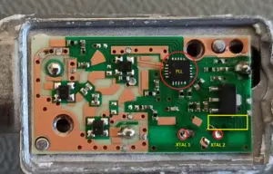
This article shows how to modify an inexpensive LNB to accept an external LO-reference signal in order to be used as a K-band downconverter for QO-100 (Qatar Es’hail 2) amateur radio sattelite reception, radio astronomy or similar K-band experiments.
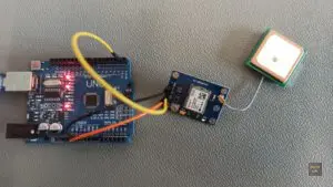
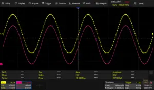
This article is a shortened version of a scientific paper that I wrote as the lead author. For a more in-depth, scientific version , feel free to download the research paper. [1]. There also is a German version of this article available: LNB Modifikation für X-Band und QO-100 Empfang

Introduction

The commercial LNB chosen here is a Goobay 67269 LNB. According to the manufacturer, the LNB is suitable for reception from 10.7 to 11.7 GHz (low-band) and from 11.7 to 12.75 GHz (high-band) [3]. The IF frequency range is 950 MHz to 1950 MHz (low-band) and 1100 to 2150 MHz (high-band). This corresponds to a local-oscillator (LO) frequency of 9.75 GHz (low-band) and 10.6 GHz (high-band).

Unmodified Goobay 67269 LNB

Unmodified Goobay 67269 LNB

The LO signal of the LNB is referenced to a 25 MHz crystal. In low-band operation, the 25 MHz is multiplied by a factor of 390, in high-band operation the multiplication factor is 424. While a standard 25 MHz crystal reference is stable enough for broadband satellite TV reception, it is insufficient for the reception of narrow-band signals commonly found on radiocommunication satellites such as the popular, geostationary QO-100 (Qatar Es’hail 2). Therefore, the desire arises to lock the LO to an externally provided reference.

This also opens up the possibility to change the LO-frequency so that the IF-frequency range can be moved to a more convenient range. For instance, the narrow-band transponder of QO-100 has a downlink frequency range of 10489.5 to 10490 MHz. The standard LO-frequency of 9750 MHz results in an intermediate frequency (IF) frequency range of 739.5 to 740 MHz. If the reference frequency is changed to 25.780 – corresponding to a LO-frequency of 10054.20 MHz -, the resulting IF frequency range would move to 435.30 MHz – 435.80 MHz, right in the center of the 70 cm amateur radio band.

Modification

The modification itself is quite simple. In essence, the 25 MHz crystal is removed and replaced by a 25 MHz LC-series resonant circuit with bandpass characteristic connected to the F-connector of the LNB. Standard component values of 18 pF and 2,2 µH were chosen for the series LC circuit.

(1)   \begin{equation*}  Z_{LC} = |2 \pi f L - \frac{1}{2 \pi f C}|  \end{equation*}

This in an impedance of 8.1 Ω at a frequency of 25 MHz. At 26 MHz the resulting impedance is 19.32 Ω, at 27 MHz this value further increases to 45.74 Ω (Eq. 1).

After removing the plastic cover using a flat screwdriver, the metal cover for the PCB housing can be removed after loosening two screws. The required screwdriver is of type Torx T8. After removal of the metal cover, the top-side of the LNB’s PCB is accessible.

Plastic cover of the LNB removed

Plastic cover of the LNB removed

Removal of the PCB housing screws

Removal of the PCB housing screws

The main function blocks of the LNB’s PCB can easily be identified. The circuit design is centered around a fully integrated PLL/LO/Downconverter-chip marked “3566E”. Even after a thorough search, very little information on this chip can be found. However, knowing the general working principle of such a chip, the relevant parts of the circuit can be reverse engineered without specific device information at hand.

The DC supply-voltage from the F-connector is passed to a 7806-type voltage regulator through a printed circuit board inductor (yellow rectangle), supplying the 3566E with stable 6 V DC. The PINS marked XTAL1 and XTAL2 connect to a 25 MHz crystal located on the backside of the PCB.

Closeup of the PCB with markings for the PLL, crystal pins and the printed circuit board inductor choke in front of the voltage regulator (yellow rectangle)

Closeup of the PCB with markings for the PLL, crystal pins and the printed circuit board inductor choke in front of the voltage regulator (yellow rectangle)

In order to identify the proper input pin for injection of an external LO-reference-signal, the waveforms on pin 1 and pin 2 where examined using an oscilloscope. Pin 2 of the 3566E (XTAL2) was consequently identified to be the most suitable pin for injection of an external reference signal.

After removal of a single solder pin right above the F-connector, the PCB can be removed from the casing. It was found to be best to apply a slight upward pressure to the PCB while heating the solder joint.

Applying slight upward pressure right next to the solder-joint

Applying slight upward pressure right next to the solder-joint

Two of the LNB PCBs before the modification (top) and after the removal of the 25 MHz crystal (bottom)

Two of the LNB PCBs before the modification (top) and after the removal of the 25 MHz crystal (bottom)

The 25 MHz, through-hole crystal on the back of the PCB was removed using a soldering iron and solder wick. A 2.2 µH inductor was then installed instead of the previously removed crystal. In order to protect the leads of the inductor from unintended contact with the grounded enclosure, it was covered with a small piece of Kapton tape. The PCB was then re-installed inside the metal enclosure and soldered back in place.

2.2 µH inductor installed in lieu of the removed 25 MHz crystal

2.2 µH inductor installed in lieu of the removed 25 MHz crystal

The now unnecessary and hindering PCB trace connecting the crystal socket pin previously described as “XTAL 1” and the 3566E PLL was cut using a sharp object. Lastly, the 18 pF capacitor has been soldered between the input connection pin (from the F-connector) and XTAL 1.

The PCB-trace connected to pin XTAL 1 has been cut using a sharp tool

The PCB-trace connected to pin XTAL 1 has been cut using a sharp tool

A 18 pF capacitor has been installed between the F-connector input pin and the XTAL 1 pin, connecting directly to the 2.2 µH inductor

A 18 pF capacitor has been installed between the F-connector input pin and the XTAL 1 pin, connecting directly to the 2.2 µH inductor

Test and Results

In order to test the functionality of the performed modification, the LNB was connected to a makeshift diplexer with integrated bias tee. Absolutely no care was taken to match the LNB’s input impedance of 75 Ω to the 50 Ω impedance of the equipment used in this test.

The high-pass path of the diplexer (fc = 100 MHz) was connected to a RTL2832 SDR through a 10 dB attenuator. The low-pass path of the diplexer (fc = 30 MHz) was connected to a signal generator. The signal generator was then set to a frequency of 25.78 MHz, resulting in a LO-frequency of 10054.2 MHz if locked on correctly. 14 VDC were then supplied to the LNB through the bias tee of the diplexer. It was observed that the LNB draws a current of 60 mA when unlocked. This value jumps to approx. 90 mA when the PLL has properly locked onto the external reference signal. Lock was observed at a signal amplitude of 3 Vpp into the diplexer. At 75 Ohms, this corresponds to a drive level of around 12 dBm.

Two signals of 3496 MHz and $3496.333 MHz were generated using an ADF4351 evaluation board from Analog Devices. The third harmonics of said signals should produce suitable test signals with frequencies of 10.488 GHz and 10.489 GHz. The ADF4351 evaluation board was set to hop between both frequencies at a rate of 500 ms.

LNB ignal output viewed in SDRSharp

LNB signal output viewed in SDRSharp

The resulting output spectrum was viewed in AirSpy SDR# Studio. The two test signals were clearly visible and the alternating 500 ms hops confirmed their identity. It was noted that due to the high gain of the LNB, it was very easy to overdrive the LNB. Despite using the third harmonic of signals with an amplitude of -4 dBm, the LNB had to be pointed away from the signal source in order not to cause distortion. Further, the 10 dB attenuator in front of the RTL2832 SDR was absolutely necessary in order not to exceed the full-scale dynamic range of the receiver.

It was further observed that varying the frequency of the reference signal between 24 MHz and 27 MHz does indeed change the LO-frequency without a visible change in IF output power or spurious frequency components.

Conclusions

This article shows that it is possible to successfully modify an inexpensive Goobay 67269 LNB to accept an external reference signal. Furthermore, the experiments shown demonstrate that the LNB is capable of down-converting K-band signals outside of the manufacturer’s specified frequency range.

Links and Sources:
[1] Westerhold, S. and Matlinski, C., “Modification of a Goobay 67269 LNB for use in 10 GHz communication satellite reception”, Jul. 2023, doi: 10.5281/zenodo.8102235.

[2] Armin Duft. “Goobay 67269 LNB Modification”. In: (2019). url: https://dh1da.darc.de/projekte/Amateurfunk/QO-100_LNB/Goobay_67269_LNB_Mod-DH1DA.pdf (visited on 07/01/2023).

[3] Wentronic GmbH. Universal Single LNB | Wentronic. url: https://www.wentronic.com/de/universal-single-lnb-67269 (visited on 07/01/2023).