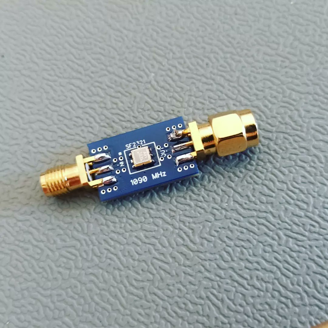
SAW filter PCB with SMA connectors for 1090 MHz (ADS-B). Mismatched input and output traces (Z=100 Ohms, l=3,5mm) have been deemed acceptable.
Rule of Thumb
Rules of thumb are made to simplify our everday engineering life. For the critical length of a PCB trace, there are various different rules of thumb available. One of those rules is the 1/10 rule (Eq. 1). It basically states that the critical length for a PCB trace is 1/10th of the wavelength. It suggests that for length smaller than 1/10 of a wavelength, any impedance (mis)match and transmission line effects can safely be ignored.
(1) 
The  term in the equation corrects for the difference between physical length and electrical length. is equal to the relative permittivity, also oftentimes called the dielectric constant (Dk), of the PCB material used. For FR4 this varies between about 4.3 and 4.5.
  is of course the wavelength as defined by the speed of light divided by the frequency.
When working with digital singals, the critical length is expressed as a function of the rise or fall time(Eq. 2).
(2) 
Where t denotes the rise- or fall-time (whichever is smaller) and  the speed of light.
Now that we have commonly accepted rules of thumb and can easily calculate the length of a PCB trace below which we can safely ignore pesky things such as impedance matching and the relative permittivity of the PCB material used, I could wrap up this article and just leave it at that, right? Unfortunately, no…
What exact fraction of a wavelength to consider to be the threshold for the critical PCB-trace length varies by literature and people’s personal preferences. There’s also the 1/4, 1/8, 1/16 and 1/20 rule and many more. So which one of these is correct and which one should you use?
Transmission Line Math
To the question of when a PCB trace should be regarded as a transmission line, the short answer is: Always! To answer the question of when it really matters, we will have to dive a little bit into the science involved. Equation 2 shows the complex input impedance ( ) of any stripline of length l in metres.
  is the characteristic impedance of the transmission line itself, in this case the PCB trace.
  is the propagation constant with the peculiar unit of radians per metre (Eq. 4).
  denotes the load impedance present at the end of the transmission line.
(3) 
(4) 
The abomination of an equation can be simplified very slightly if the length l is given as a factor relative to the wavelength, for instance 0.25 or 1/4 for a quarter wavelength (Eq. 5).
(5) 
From this equation it is apparent that there is only a single case where the length of the PCB trace doesn’t matter. And that is when = . Or in other words when the trace impedance perfectly matches the load impedance, for instance 50 Ohms. Under any other condition, except at length 0 (and multiples of 1/2 wavelength), the trace impedance will have some influence on the impedance seen at the beginning of the trace. But by how much and how much is acceptable?
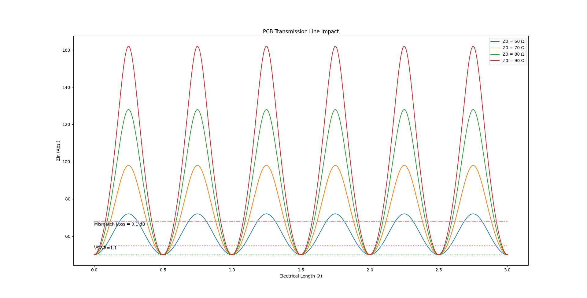
A picture is worth a thousand words as they say. Let’s assume a load impedance of 50 Ohms and arbitrarily pick mismatched trace impedances of 60, 70, 80 and 90 Ohms. Using equation 4, the impedance seen at the beginning of the trace can be plottet as a function of electrical length.
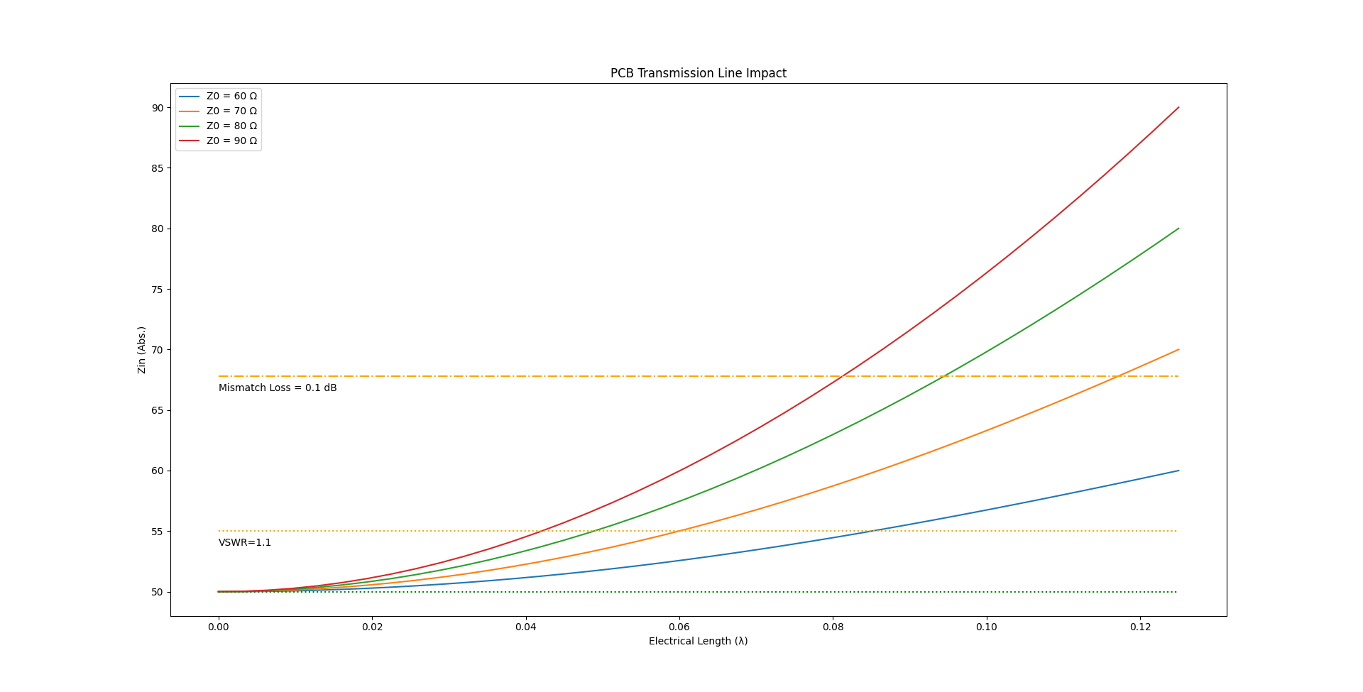
Input impedance as a function of electrical length and trace-impedance.
Just for fun, I also plottet the same function with trace impedances of 20, 35, 65 and 80 Ohms. However, a smaller characteristic impedance of a PCB trace means that it is too wide. In that instance, honestly, just make it thinner and match it to 50 Ohms. Because the usual case of why we even might want to ignore impedance matched traces is because of their width. Especially in home made projects or when using one’s favorite chinese PCB manufaturer, the default PCB material is 1.6mm thick FR4. Assuming a dielectric constant of roughly 4.3, a microstripline with a characteristic impedance of 50 Ohms would have a thickness of around 3.1 mm. Using just 1mm thick FR4 with the same dielectric constant would reduce this to a more acceptable 2mm. Additionally, FR4 has the tendency to not have a very well controlled dielectric constant.
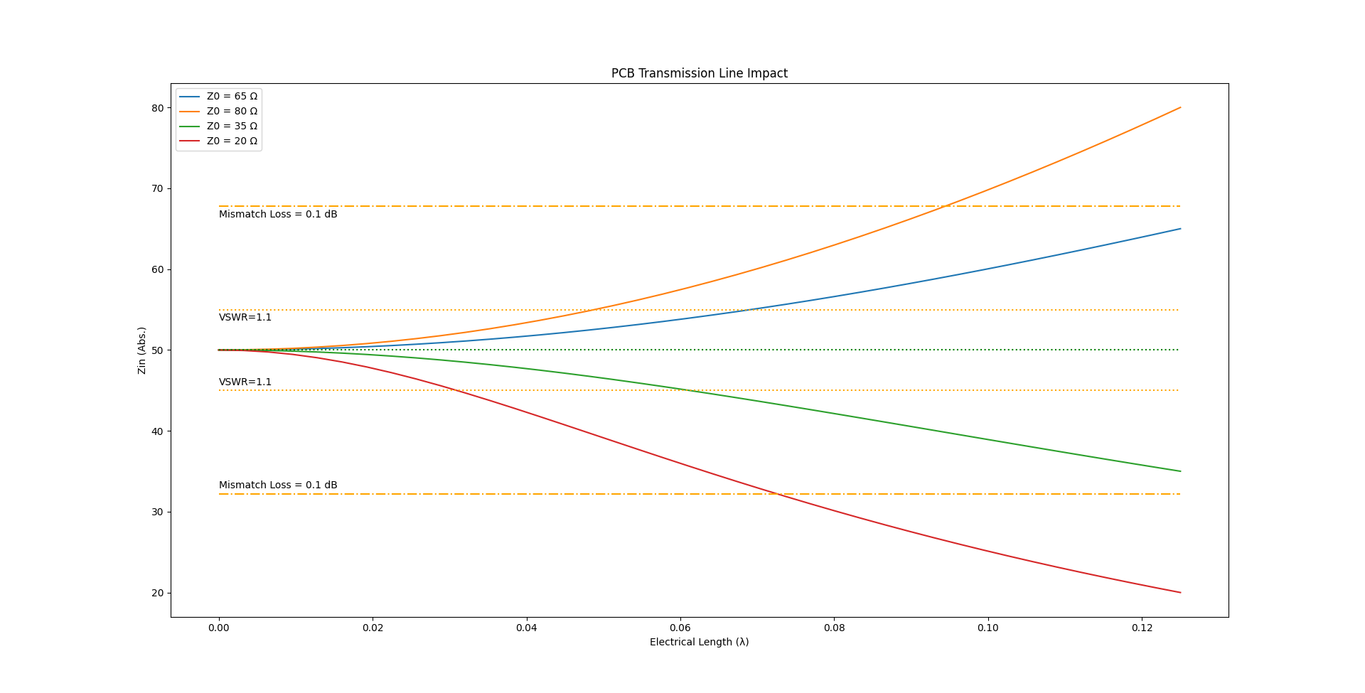
Input impedance as a function of electrical length and trace-impedance.
The previous graphs confirm what the math already showed: Any length (except 0) of a mismatched PCB trace has an influence on the input impedance of the trace. To decide what is acceptable and what not, we have to define what we will accept in our designs. Two possible figures of merit vould be the VSWR or the mismatch loss. The mismatch loss indicates how much of the input power is lost due to the impedance mismatch. I included two horizontal lines enclosing a VSWR of < 1:1.1, which corresponds to a mismatch loss of 0.01 dB. Another pair of horizontal lines marks the area in which the mismatch loss is below 0.1 dB, corresponding to a VSWR 1:1.356. At a VSWR of 1:1.356, 97.72 % of the transmitted power reaches the load, 2.28 % get reflected back to the load. At a VSWR of 1:1.1, these values improve to 99.77 % forward power and 0.23 % reflected power.
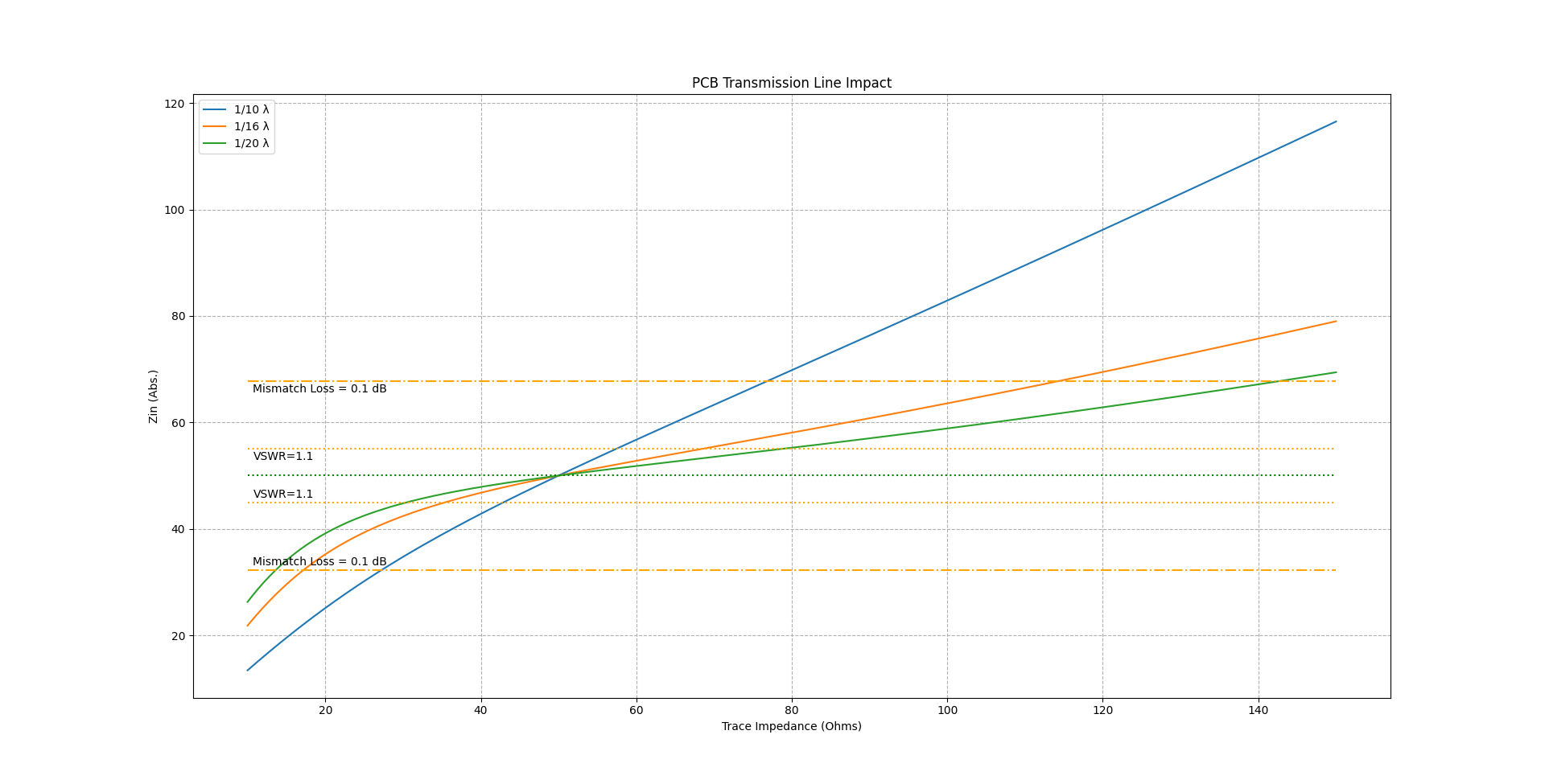
Input impedance plottet as a function of trace impedance for trace lengths of 1/10, 1/16 and 1/20 of a wavelength.
What you deem acceptable for your design is entirely up to you. Personally, in my hobby designs I yield for a mismatch loss of less than 0.1 dB. As shown in the graph, using the 1/10 rule of thumb will quickly put the design outside of those limits. The 1/16 rule (Eq. 6), however, is a really good and useful approximation. At least for PCB traces with a characteristic impedance of less than 110 Ohms. By simply keeping all relevant traces wider than 0.75 mm (max. Z ~100 Ohms, FR4, Dk=4.3, PCB thickness=1.6mm) I effectively eradicate the need to double check the trace impedance in addition to the critical length.
(6) 
The periodicity of the input impedance at 1/2 wavelength intervals is also an interesting phenomenon. Half a wavelength corresponds to 180 degrees of phase shift. For a reflected signal the total round trip delay would thus be 360 degrees. Assuming a periodic signal, the reflected signal would thus be in phase with the “new” signal at the input. Therefore, one could theoretically intentionally design a mismatched transmission line with a total length less than the critical length plus any integer multiple of 1/2 .
Periodicity of the input impedance of a mismatched transmission line as a function of electrical length
Conclusions
Within certain constraints, rules of thumb can be an effective guide to estimate the critical length of a PCB trace. However, it is important to be aware of one’s own design requirements and not be tempted to completely ignore any transmission line effects regardless of length.
Westerhold, S. (2023), "Critical length of a PCB trace and when to treat it as a transmission line". Baltic Lab High Frequency Projects Blog. ISSN (Online): 2751-8140., https://baltic-lab.com/2023/08/critical-length-of-a-pcb-trace-and-when-to-treat-it-as-a-transmission-line/, (accessed: July 10, 2026).

- Conducted Emissions on the Bench: Implementing the CISPR 25 Voltage Method - December 15, 2025
- WebP-Images without Plugin - January 14, 2025
- Firewall Rules with (dynamic) DNS Hostname - January 14, 2025