Introduction
When using modified, commercial LNBs for reception of the QO-100 amateur radio satellite or X-band microwave experiments, it is necessary to pass a clock-reference signal, a DC supply voltage and the receive IF signal through the same coax. It is, therefore, necessary to separate these signals at the other end of the coax. For that purpose a Diplexer for IF / clock-reference separation plus an additional Bias-T is needed. Additionally, the LNBs are designed for a typical systems impedance of 75 Ohms instead of the 50 Ohms commonly used in RF communications equipment. An ideal Diplexer with integrated bias-T, which I will call a Triplexer from now on, also takes care of the impedance matching.
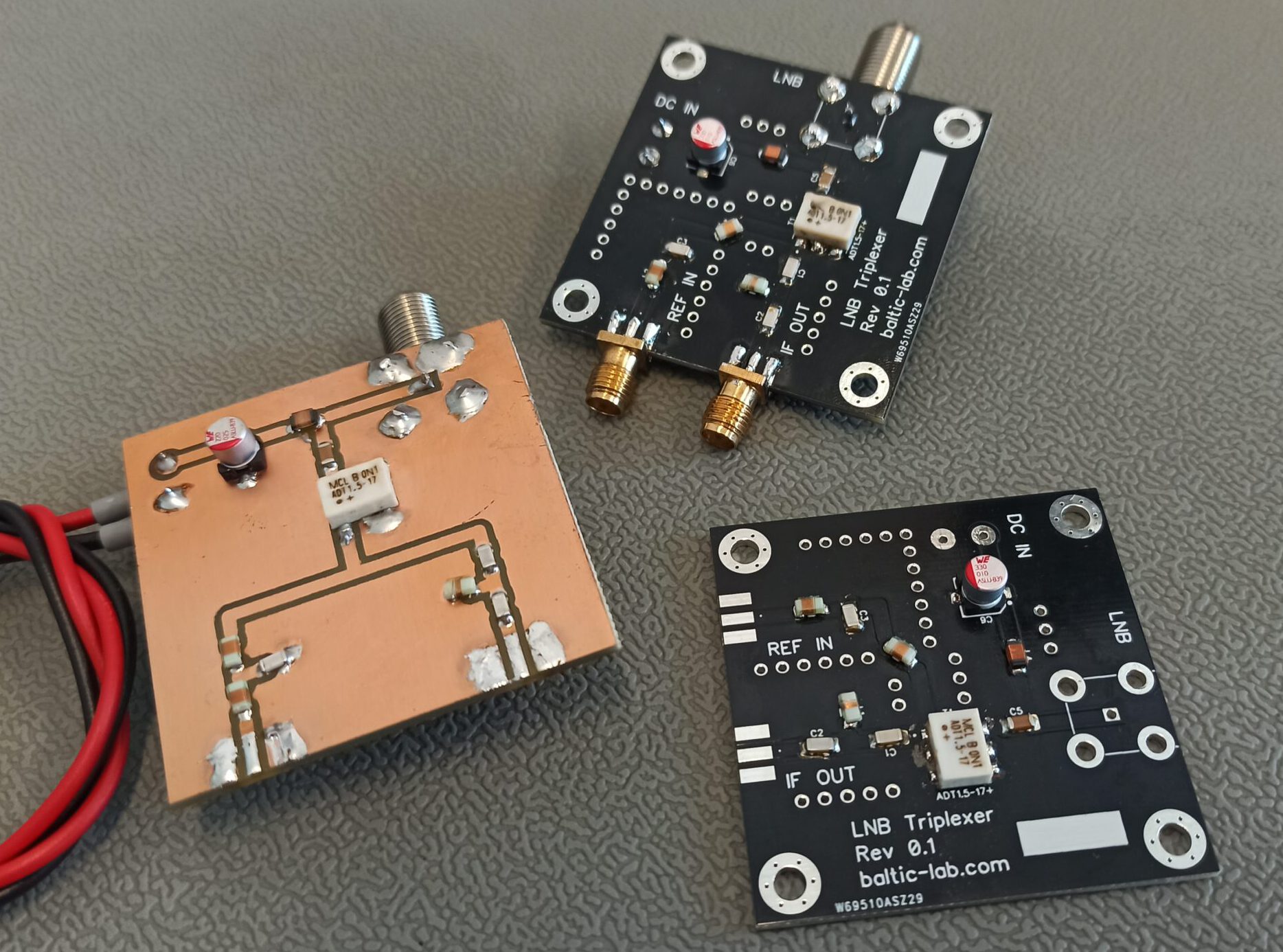
Different PCB prototype versions of the Diplexer with integrated bias-T
Circuit Design
For the Intermediate Frequency (IF) and clock-reference separation, the circuit makes use of two T-type LC-networks. Their corner frequencies are calculated in a way that even reception on the 2m amateur radio band would be possible on the IF-side of the setup. The additional benefit of the low-pass characteristic of the T-network on the clock-reference side is that a reference square wave will effectively be turned into a sine-wave. Therefore, square wave shaped clock signal sources can be used.
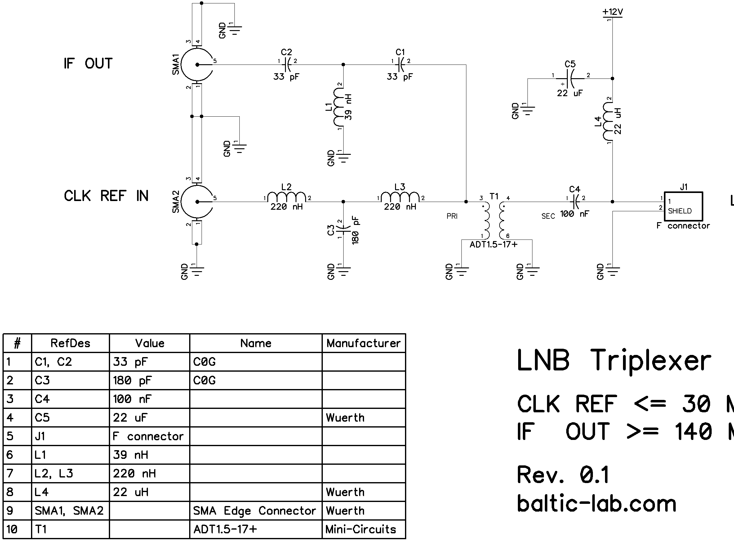
Schematic of the LNB Triplexer (Diplexer with integrated Bias-T) for use in QO-100 reception and X-band microwave receive setups.
The IF and reference-clock nodes are then combined and sent to the primary side of a MiniCircuits ADT1.5-17+ transformer with an impedance transformation ratio of 1:1.5 [1]. The secondary side of the transformer (now 75 Ohm impedance) is isolated from the DC bias-T by a simple blocking capacitor. The bias-T itself, consisting out of C5 and L4, is a simple LC-low-pass filter. The combined signal-path from the secondary side of T1 and the supply voltage from the bias-T are combined and connected to an F-type output connector.
For C1, C2 and C3 no capacitors with class 2 dielectric are recommended. C0G or NP0 type capacitors are recommended to provider more stability of the passband characteristics of the T-filters.
PCB Design
Except for the RF-connectors and the DC input terminal, all components are surface mount devices. By using mostly 1206 footprint passive components, this is still extremely easy to assemble at home. The PCB layout is intended for standard 1.6mm thick FR4 material and a . The general design-considerations regarding impedance matching of PCB traces, or rather to what extend it is even necessary, from my article “Critical length of a PCB trace and when to treat it as a transmission line” [2 have been applied in this design. For that reason, the IF portion is situated a lot closer to the primary side of the transformer than the reference-clock input.
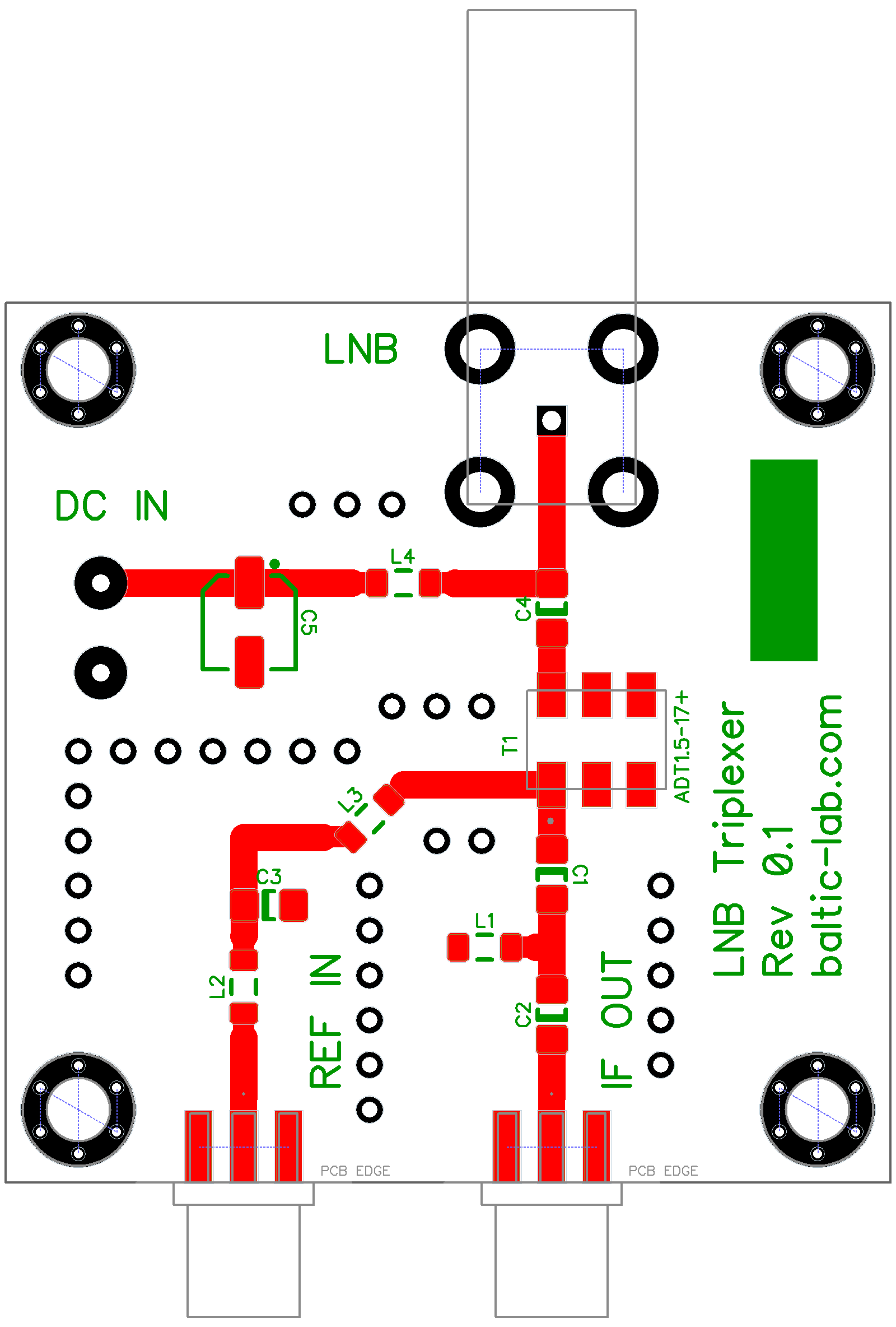
PCB design with part markings, without copper pur (for better visibility) for the Triplexer.
The PCB features two edge-mount SMA connectors for the reference-clock input and the IF output. The DC supply voltage can be applied using 2,54 mm screw terminals. Care has been taken to orient all inductors in a way that coupling of their magnetic fields is reduced to a minimum.
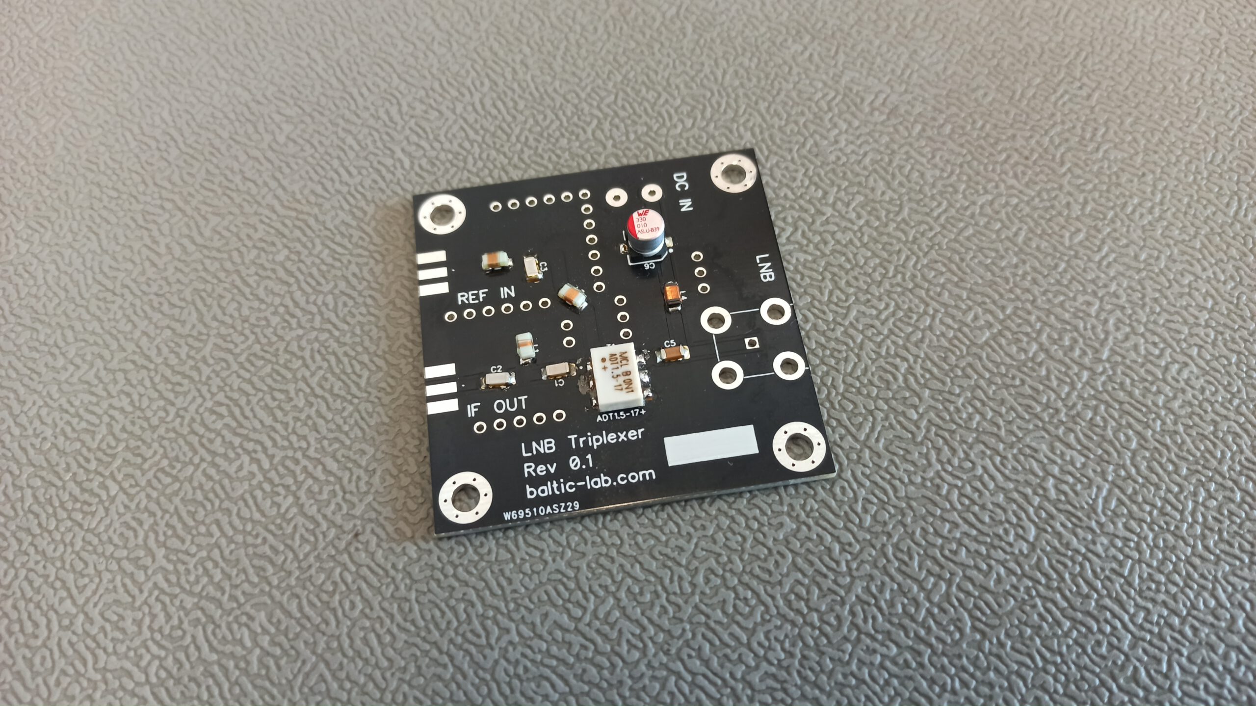
Triplexer PCB with all components except the connectors assembled.
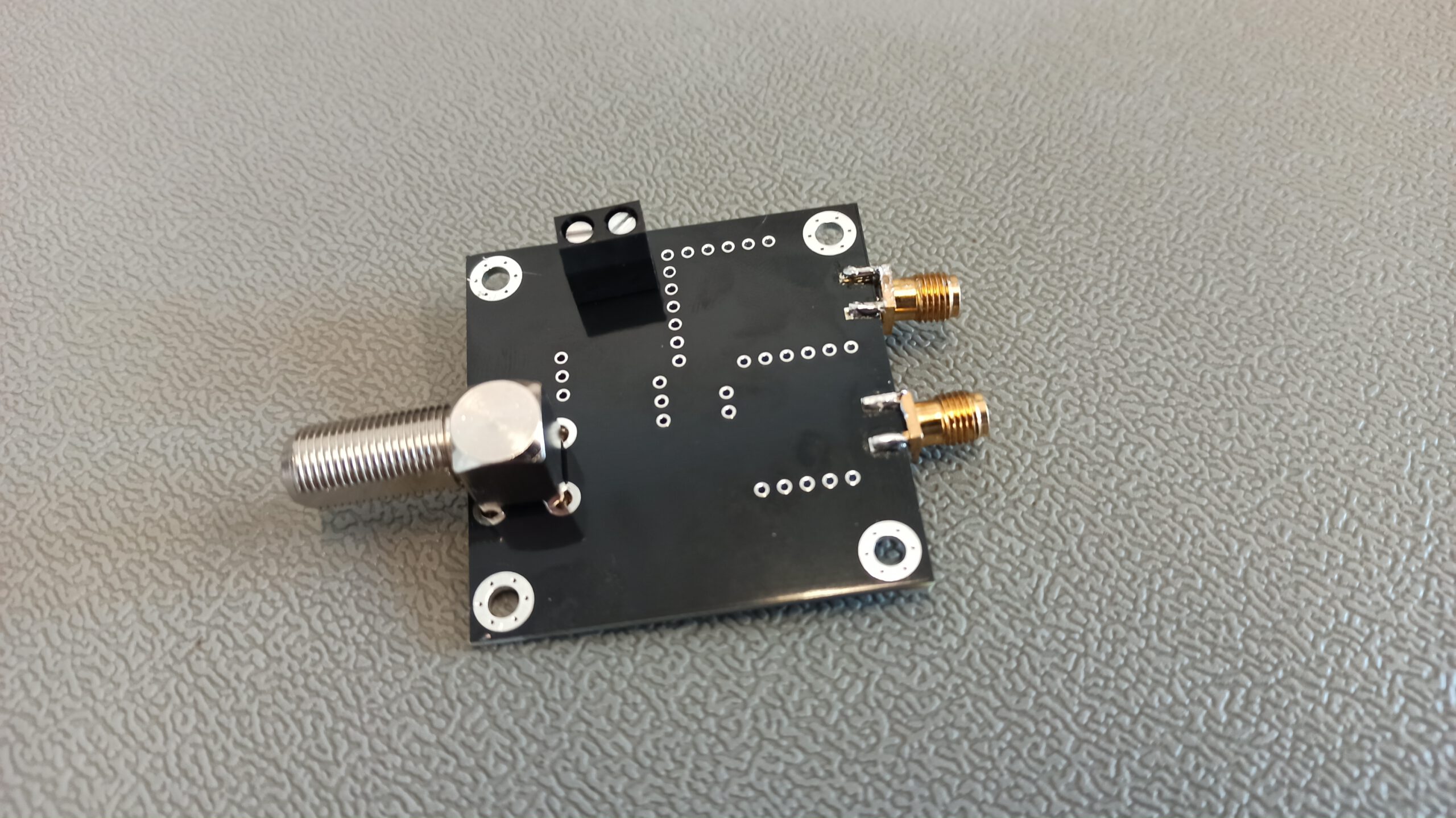
Backside of the Triplexer PCB with F-type connector for the LNB-syde, edge mount SMA connectors and screw terminal for the DC supply voltage
Test Results
For a subjective, general function test, modified Goobay 67269 LNB [3] was used for initial testing. The LNB was connected to the F-connector using a few metres of 75 Ohm coax. As a test signal source with a frequency of 10.488 GHZ, the 23rd harmonic of a 456 MHz signal (Po = 500 mW) from a handheld radio was used. The LO frequency was set to 10 GHz by injecting a reference-clock frequency 25.641025 MHz.
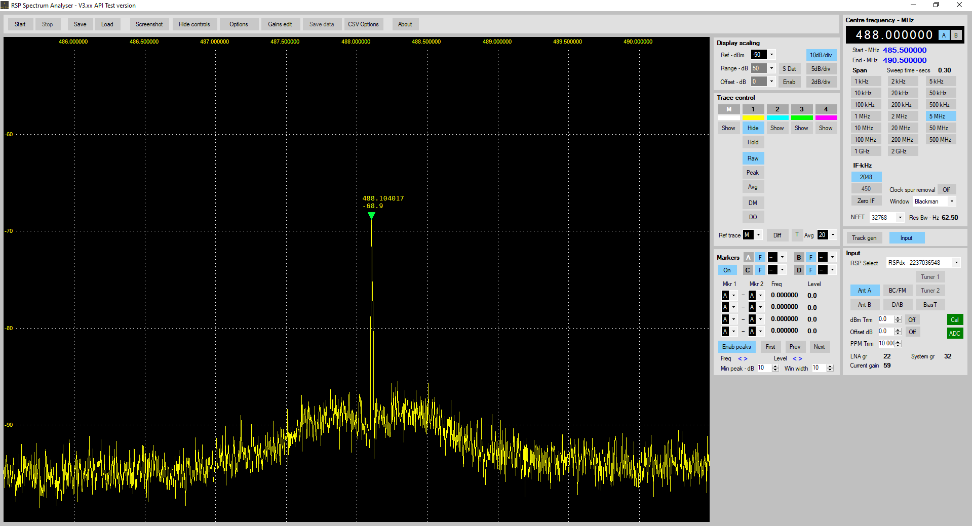
Output from the IF port viewed on a SDRPlay RSPdx, reference input frequency 10.488 GHz, reference clock input = 25.641025 MHz
It should be noted that for this prototype test, I deviated from the calculated component values. 270 nH inductors where used in Place of the 220 nH inductors (L2 and L3)and some deviation was also on the IF-side, but I can’t really remember what capacitor values were actually used. I will update the figures once I have the updated prototype revision with the correct component values assembled. Nonetheless, port characteristics were measured with a NanoVNA.
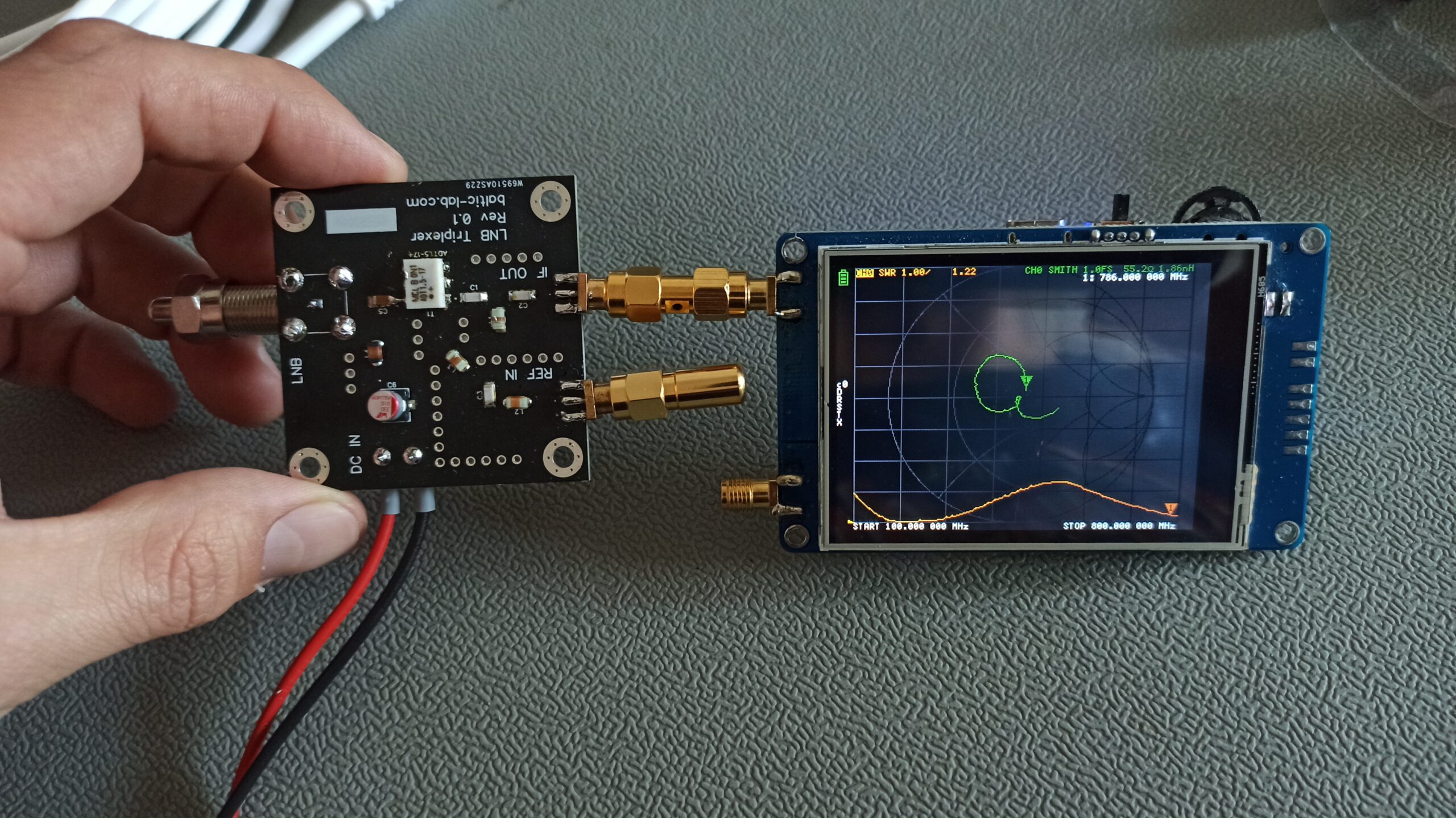
Nano VNA used to verify the port characteristics of the IF port. The LNB port and the reference clock port are properly terminated with a 75 Ohm (LNB) and 50 Ohm load (reference clock).
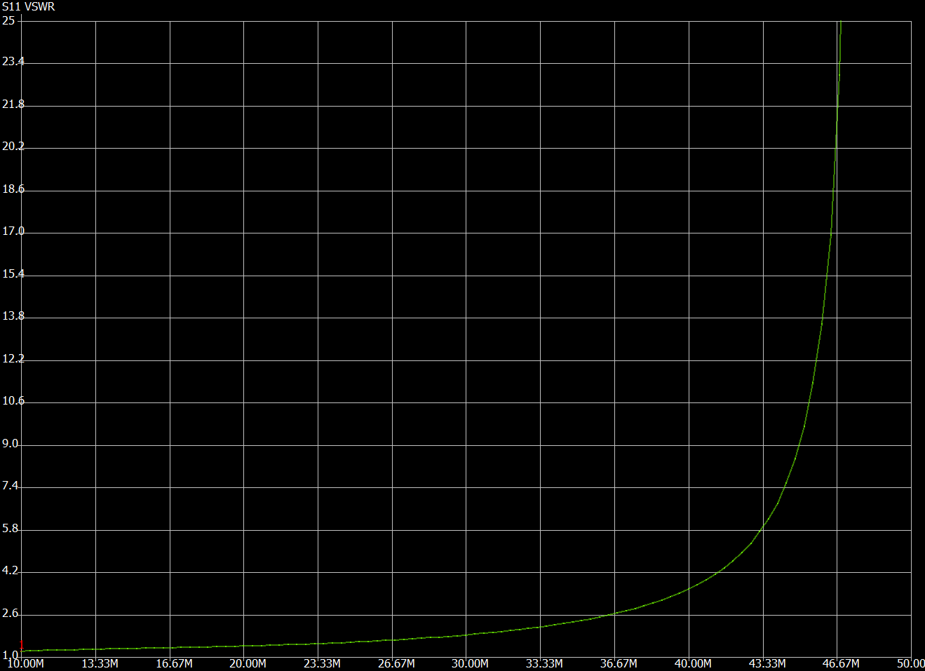
To measure the input VSWR of the IF port, the LNB connector was properly terminated with a 75 Ohm load. The reference clock input was terminated with a 50 Ohm load. The resulting VSWR-plot is okay, but I’d like to see better results than that.
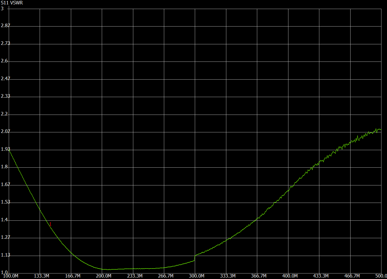
S11 VSWR of the IF port with all other ports properly terminated.
The test was repeated on the reference-clock port by connecting the NanoVNA to the reference-clock input port and terminating the IF port with a 50 Ohm load. The result is acceptable but should be re-verified with the next revision.
Reference clock input port VSWR measurement with all other ports properly terminated.
Conclusions
This article shows a simple design approach on how to implement a functional triplexer design for QO-100 reception and X-band microwave experiments using with a modified LNB. Some improvements will be implemented in the next revision, such as a larger power inductor being able to handle higher supply currents. When the next revision becomes available, I will update this article to provide measurements and the design-files (Gerber and drill files).
Links and Sources:
[1] ADT1.5-17+ Datasheet, MiniCircuits: https://www.minicircuits.com
[2] Westerhold, S. (2023), “Critical length of a PCB trace and when to treat it as a transmission line”. Baltic Lab High Frequency Projects Blog. ISSN (Online): 2751-8140.: https://baltic-lab.com
[3] Westerhold, S. (2023), “LNB Modification for 10 GHz QO-100 Satellite Reception”. Baltic Lab High Frequency Projects Blog. ISSN (Online): 2751-8140.: https://baltic-lab.com
Westerhold, S. (2023), "Diplexer with integrated Bias-T (Triplexer) for QO-100 and X-band microwave reception using LNBs". Baltic Lab High Frequency Projects Blog. ISSN (Online): 2751-8140., https://baltic-lab.com/2023/08/diplexer-with-integrated-bias-t-triplexer-for-qo-100-and-x-band-microwave-reception-using-lnb/, (accessed: July 23, 2026).

- Conducted Emissions on the Bench: Implementing the CISPR 25 Voltage Method - December 15, 2025
- WebP-Images without Plugin - January 14, 2025
- Firewall Rules with (dynamic) DNS Hostname - January 14, 2025