Automated Forward Gain Measurement
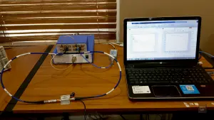
This article is going to take you into the world of automation. Using MATLAB and commercial off-the-shelf bits and pieces, this article will show how to measure the forward gain of a RF device.
This article is going to take you into the world of automation. Using MATLAB and commercial off-the-shelf bits and pieces, this article will show how to measure the forward gain of a RF device.
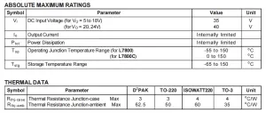
Thermal design is one of those things engineers don’t really learn in school and hobbyists often don’t even think about. This article is going to show some basic math with a practical example. One of my portable police scanners has an external 6V jack. To use it in my car I used my standard linear … [Read more…]
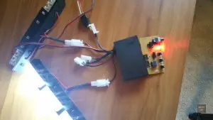
Not too long ago I bought some white strobe lights with a strobe controller of Amazon. This exact controller is spread all over Amazon and eBay but only provides strobe patterns that I didn’t particularly like. So it’s time for a hack. The strobe lights I purchased were white in color but they have the … [Read more…]
Quick introduction to Secondary Surveillance Radar and how it works. After explaining the absolute basics, I am showing how one can simulate transponder responses using off-the-shelf test equipment. RTL1090 is used to verify the generated signals as valid. If you want the arb waveform file for the 7777 Mode A response, here it is: https://baltic-lab.com/wp-content/uploads/2015/12/SQUAWK_7777_IDENT.zip
Quick look both at & inside the brand new Tektronix TSG4106 6 GHz vector signal generator. They say real beauty lies on the inside and this beauty certainly measures up, inside and out.